# A B C D E F G H I J K L M N O P Q R S T U V W X Y Z

National Semiconductor ADC0820 8-Bit High-Speed μP-Compatible A/D Converter with Track-Hold Function

Summary

The ADC0820 is an 8-Bit High Speed Analog-to-Digital Converter designed for microprocessor compatibility. Featuring built-in track/hold functionality and fast conversion times (1.5 μs), it simplifies data acquisition using a single supply voltage (0V to 5V). This product guide provides comprehensive technical specifications, operating parameters, power consumption details, and interface diagrams necessary for integration into embedded systems. Ideal for hardware engineers and designers developing reliable and high-performance analog measurement circuitry.
📄 Preview PAGE OF 22

Page 1 Text Content

查询ADC0820BCN供应商

8-B it igh peed µP om patible /D onverter ith Track/H old Function

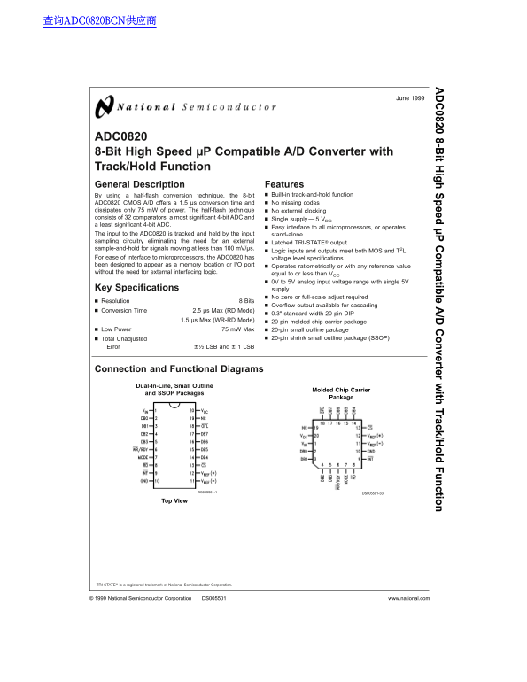
ADC0820 8-Bit High Speed µP Compatible A/D Converter with Track/Hold Function General Description Features

By using half-flash conversion technique, the 8-bit Built-in track-and-hold function

ADC0820 CMOS A/D offers 1.5 µs conversion time and No missing codes dissipates only m W of power. The half-flash technique No external clocking consists of comparators, most significant 4-bit ADC and Single supply VDC least significant 4-bit ADC.

Easy interface to all microprocessors, or operates

The input to the ADC0820 is tracked and held by the input stand-alone sampling circuitry eliminating the need for an external

Latched TRI-STATE® output

sample-and-hold for signals moving at less than m V/µs.

Logic inputs and outputs meet both MOS and T2L

For ease of interface to microprocessors, the ADC0820 has voltage level specifications been designed to appear as memory location or I/O port

Operates ratiometrically or with any reference value

without the need for external interfacing logic.

equal to or less than VCC 0V to 5V analog input voltage range with single 5V

Key Specifications supply

No zero or full-scale adjust required

Resolution Bits

Overflow output available for cascading

Conversion Time 2.5 µs Max (RD Mode)

0.3" standard width 20-pin DIP

1.5 µs Max (WR-RD Mode) 20-pin molded chip carrier package

Low Power m W Max 20-pin small outline package

Total Unadjusted 20-pin shrink small outline package (SSOP)

Error ±1⁄2 LSB and LSB

Connection and Functional Diagrams

Dual-In-Line, Small Outline

Molded Chip Carrier

and SSOP Packages

Package

DS005501-1 DS005501-33

TRI-STATE® is registered trademark of National Semiconductor Corporation.

National Semiconductor Corporation DS005501 www.national.com

Page Summary Contents For National Semiconductor ADC0820 8-Bit High-Speed μP-Compatible A/D Converter with Track-Hold Function

Page 1 查询ADC0820BCN供应商 8-B it igh peed µP om patible /D onverter ith Track/H old Function ADC0820 8-Bit High Speed µP Compatible A/D Converter with Track/Hold Function General Description Features By using h...
Page 2 Connection and Functional Diagrams (Continued) DS005501-2 FIGURE 1. Ordering Information Part Number Total Package Temperature Unadjusted Error Range ADC0820BCV V20A Molded Chip Carrier 0˚C to +70˚C A...
Page 3 Absolute Maximum Ratings (Notes 1, 2) Dual-In-Line Package (ceramic) 300˚C If Military/Aerospace specified devices are required, Surface Mount Package please contact the National Semiconductor Sales O...
Page 4 DC Electrical Characteristics The following specifications apply for VCC=5V, unless otherwise specified. Boldface limits apply from TMIN to TMAX; all other limits TA=TJ=25˚C. Parameter Conditions ADC0...
Page 5 AC Electrical Characteristics (Continued) The following specifications apply for VCC=5V, tr=tf=20 ns, VREF(+)=5V, VREF(−)=0V and TA=25˚C unless otherwise speci- fied. Typ Tested Design Parameter Condi...
Page 6 TRI-STATE Test Circuits and Waveforms DS005501-4 DS005501-3 tr=20 ns DS005501-6 tr=20 ns DS005501-5 Timing Diagrams DS005501-7 Note: On power-up the state of INT can be high or low. FIGURE 2. RD Mode ...
Page 7 Timing Diagrams (Continued) DS005501-8 FIGURE 3. WR-RD Mode (Pin is High and t RD<t I) DS005501-9 FIGURE 4. WR-RD Mode (Pin is High and t RD>t I) DS005501-10 FIGURE 5. WR-RD Mode (Pin is High) S...
Page 8 Typical Performance Characteristics Logic Input Threshold Conversion Time (RD Mode) Power Supply Current vs Voltage vs Supply Voltage vs Temperature Temperature (not including reference ladder) DS0055...
Page 9 Description of Pin Functions Pin Name Function INT WR-RD Mode Pin Name Function INT going low indicates that the VIN Analog input; range =GND≤VIN≤VCC conversion is completed and the data DB0 TRI-STATE...
Page 10 1.0 Functional Description by connecting the second input on each capacitor and open- (Continued) ing all of the other switches (S switches). The change in volt- ladder for the A/D as well as for gene...
Page 11 1.0 Functional Description conversion time is desired, the processor need not wait for (Continued) INT and can exercise read after only ns (Figure If sured while WR is low. In RD mode, sampling occurs...
Page 12 1.0 Functional Description (Continued) DS005501-20 Note: MS means most significant LS means least significant FIGURE 11. Operating Sequence (WR-RD Mode) OTHER INTERFACE CONSIDERATIONS Since the MS fla...
Page 13 Detailed Block Diagram DS005501-15 FIGURE 12. www.national.com13
Page 14 The equivalent input circuit of the ADC0820 is shown in Fig- 2.0 Analog Considerations ure 14. When conversion starts (WR low, WR-RD mode), all input switches close, connecting VIN to thirty-one p F c...
Page 15 2.0 Analog Considerations 2.4 INHERENT SAMPLE-HOLD (Continued) Another benefit of the ADC0820’s input mechanism is its ability to measure variety of high speed signals without the help of an external ...
Page 16 3.0 Typical Applications 8-Bit Resolution Configuration DS005501-26 9-Bit Resolution Configuration DS005501-27 www.national.com
Page 17 3.0 Typical Applications (Continued) Telecom A/D Converter Multiple Input Channels DS005501-28 VIN=3 k Hz max 4VP DS005501-29 No track-and-hold needed Low power consumption 8-Bit 2-Quadrant Analog Mul...
Page 18 3.0 Typical Applications (Continued) Fast Infinite Sample-and-Hold DS005501-31 www.national.com
Page 19 3.0 Typical Applications (Continued) ig it al av ef rm ec rd er www.national.com19
Page 20 Physical Dimensions inches (millimeters) unless otherwise noted Hermetic Dual-In-Line Package (J) Order Number ADC0820CCJ NS Package Number J20A www.national.com
Page 21 Physical Dimensions inches (millimeters) unless otherwise noted (Continued) SO Package (M) Order Number ADC0820BCWM, ADC0820CCWM or ADC0820CIWM NS Package Number M20B Molded Dual-In-Line Package (N) O...
Page 22 8- it ig pe ed µP om pa tib le /D on ve rt er ith Tr ac k/ ol Fu nc tio Physical Dimensions inches (millimeters) unless otherwise noted (Continued) Molded Chip Carrier Package (V) Order Number ADC0820...

Manual Details

Brand National
Pages 22
File Size 484.43 KB
Published May 27, 2026
100 views

Enter the captcha to get the download link:

captcha

Frequently Asked Questions

What voltage supply does the ADC0820 require for operation?

It requires a single 5 V DC supply.

How fast can the device achieve conversion time in WR-RD mode?

The maximum conversion time is 1.5 μs.

What are the acceptable analog input voltage ranges?

The allowable analog input range is from 0V to 5V.

Can this converter easily connect with standard microprocessors?

Yes, its logic inputs and outputs meet both MOS and TTL specifications for easy interface.