National Semiconductor ADC12DS080 Dual 12-Bit, 80 MSPS A/D Converter with Serial LVDS Outputs
Summary
The ADC12DS080 is a high-performance dual 12-Bit Analog-to-Digital Converter, offering up to 80 MSPS conversion speed for professional signal processing applications. Designed with a differential pipelined architecture and serialized LVDS outputs, it provides excellent dynamic performance while maintaining low power consumption. This manual serves as a comprehensive guide for engineers utilizing the ADC in fields such as wireless base stations, test equipment, and communications instrumentation, detailing setup, pin assignments, and complex operational modes.
Page 1 Text Content
l 1 -B it, 8 /D rte r w ith ria l L tp ts
March 6, 2008
ADC12DS080 Dual 12-Bit, 80 MSPS A/D Converter with Serial LVDS Outputs General Description Features The ADC12DS080 is a high-performance CMOS analog-to- Clock Duty Cycle Stabilizer digital converter capable of converting two analog input sig-
Single +3.0 or 3.3V supply operation
nals into 12-bit digital words at rates up to 80 Mega Samples
Serial LVDS Outputs
Per Second (MSPS). The digital outputs are serialized and
Serial Control Interface
provided on differential LVDS signal pairs. This converter us-
es a differential, pipelined architecture with digital error cor- Overrange outputs
rection and an on-chip sample-and-hold circuit to minimize 60-pin LLP package, (9x9x0.8mm, 0.5mm pin-pitch) power consumption and the external component count, while providing excellent dynamic performance. The ADC12DS080
Key Specifications
may be operated from a single +3.0V or 3.3V power supply.
Resolution 12 Bits
A power-down feature reduces the power consumption to
very low levels while still allowing fast wake-up time to full Conversion Rate 80 MSPS operation. The differential inputs accept a 2V full scale differ- SNR (f IN = 170 MHz) 70 d BFS (typ)
ential input swing. A stable 1.2V internal voltage reference is SFDR (f IN = 170 MHz) 81 d BFS (typ) provided, or the ADC12DS080 can be operated with an ex- Full Power Bandwidth 1 GHz (typ) ternal 1.2V reference. The selectable duty cycle stabilizer
Power Consumption 800 m W (typ)
maintains performance over a wide range of clock duty cy- cles. A serial interface allows access to the internal registers
Applications
for full control of the ADC12DS080's functionality. The AD-
C12DS080 is available in a 60-lead LLP package and oper- High IF Sampling Receivers
ates over the industrial temperature range of −40°C to +85°C Wireless Base Station Receivers
Test and Measurement Equipment Communications Instrumentation Portable Instrumentation
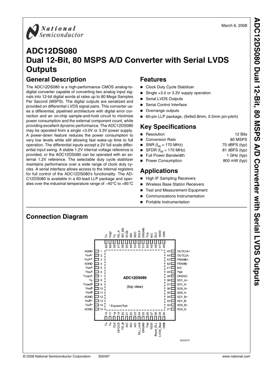
Connection Diagram
© 2008 National Semiconductor Corporation www.national.com
Page Summary Contents For National Semiconductor ADC12DS080 Dual 12-Bit, 80 MSPS A/D Converter with Serial LVDS Outputs
Manual Details
| Brand | National |
|---|---|
| Pages | 26 |
| File Size | 503.22 KB |
| Published | June 17, 2026 |
Enter the captcha to get the download link:
