National Semiconductor ADC0819 8-Bit Serial I/O A/D Converter with 19-Channel Multiplexer
Summary
The ADC0819 is a high-performance, 8-Bit successive approximation A/D converter featuring an integrated 19-Channel Multiplexer and simultaneous serial input/output capability. Ideal for engineers requiring precise analog signal acquisition up to 5V, this chip includes essential features like sample-and-hold functionality and single 5V power operation for reliable interfacing with microprocessors. This technical manual provides comprehensive specifications, detailed connection diagrams, operational ratings, and electrical characteristics necessary for successful system design and integration.
Page 1 Text Content
查询ADC0819供应商
December
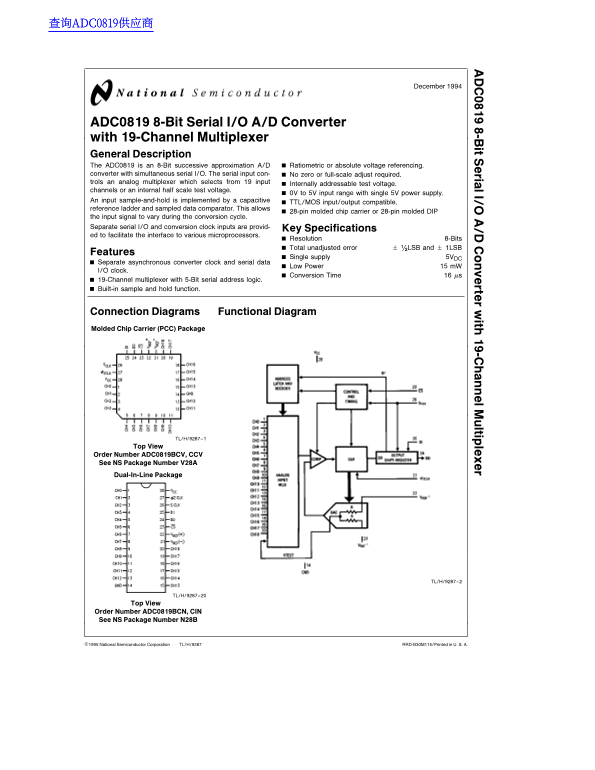
-B it ria I/ rte ith -C ltip le ADC0819 8-Bit Serial I/O A/D Converter with 19-Channel Multiplexer General Description The ADC0819 is an 8-Bit successive approximation A/D Ratiometric or absolute voltage referencing.
converter with simultaneous serial I/O. The serial input con- No zero or full-scale adjust required. trols an analog multiplexer which selects from input Internally addressable test voltage. channels or an internal half scale test voltage.
0V to 5V input range with single 5V power supply.
An input sample-and-hold is implemented by capacitive TTL/MOS input/output compatible. reference ladder and sampled data comparator. This allows
28-pin molded chip carrier or 28-pin molded DIP
the input signal to vary during the conversion cycle. Separate serial I/O and conversion clock inputs are provid- Key Specifications ed to facilitate the interface to various microprocessors.
Resolution 8-Bits Total unadjusted error (/2LSB and 1LSB
Features
Single supply 5VDC
Separate asynchronous converter clock and serial data
Low Power m W
I/O clock.
Conversion Time ms
19-Channel multiplexer with 5-Bit serial address logic. Built-in sample and hold function.
Connection Diagrams Functional Diagram Molded Chip Carrier (PCC) Package
TL/H/9287–1
Order Number ADC0819BCV, CCV See NS Package Number V28A
Dual-In-Line Package
TL/H/9287–2
TL/H/9287–20
Order Number ADC0819BCN, CIN See NS Package Number N28B
C1995 National Semiconductor Corporation TL/H/9287 RRD-B30M115/Printed in U. S. A.
Page Summary Contents For National Semiconductor ADC0819 8-Bit Serial I/O A/D Converter with 19-Channel Multiplexer
Manual Details
| Brand | National |
|---|---|
| Pages | 12 |
| File Size | 284.57 KB |
| Published | June 16, 2026 |
Enter the captcha to get the download link:

Frequently Asked Questions
What is the input range and supply voltage for this converter?
The converter supports a 0V to 5V input range using a single 5V power supply.
How many channels can I select from?
It features a multiplexer that selects from 19 input channels or an internal test voltage.
What is the maximum total unadjusted error of the ADC0819?
The typical unadjusted error specified for the ADC0819BCV/CCV and ADC0819BCN/CIN models is $\pm \frac{1}{2}$ LSB.
Can this device be used in a life support system?
No, it is explicitly noted that these national products are not authorized for use as critical components in life support devices or systems.