# A B C D E F G H I J K L M N O P Q R S T U V W X Y Z

NATIONAL SEMICONDUCTOR - ADC108S022 8-Channel, 50 kSPS to 200 kSPS, 10-Bit A/D Converter Owner's Manual, User Guide

Summary

This low-power, 10-bit, eight-channel ADC is a professional analog-to-digital converter designed to operate at rates from 50 kSPS to 200 kSPS. Equipped with independent power management and compatibility across major interfaces like SPI/QSPI™, it converts challenging analog signals into reliable digital data streams. This device is engineered for rigorous applications, providing performance stability in automotive, medical, and general industrial control systems across an extended temperature range of −40°C to +105°C.
📄 Preview 📖 Table of Contents Contents PAGE OF 17

Page 1 Text Content

September

108S 8-C hannel,50 k S to k S ,10-B it /D onverter

ADC108S022 8-Channel, k SPS to k SPS, 10-Bit A/D Converter General Description Features

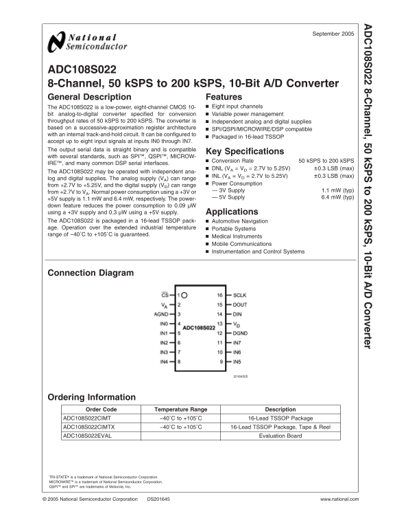
The ADC108S022 is low-power, eight-channel CMOS 10- Eight input channels bit analog-to-digital converter specified for conversion Variable power management

throughput rates of k SPS to k SPS. The converter is Independent analog and digital supplies based on successive-approximation register architecture

SPI/QSPI/MICROWIRE/DSP compatible

with an internal track-and-hold circuit. It can be configured to

Packaged in 16-lead TSSOP

accept up to eight input signals at inputs IN0 through IN7. The output serial data is straight binary and is compatible

Key Specifications

with several standards, such as SPI™, QSPI™, MICROW-

Conversion Rate k SPS to k SPS

IRE™, and many common DSP serial interfaces.

DNL (VA VD 2.7V to 5.25V) ±0.3 LSB (max)

The ADC108S022 may be operated with independent ana-

INL (VA VD 2.7V to 5.25V) ±0.3 LSB (max)

log and digital supplies. The analog supply (VA) can range

Power Consumption

from +2.7V to +5.25V, and the digital supply (VD) can range

3V Supply 1.1 m W (typ)

from +2.7V to VA. Normal power consumption using +3V or

5V Supply 6.4 m W (typ)

+5V supply is 1.1 m W and 6.4 m W, respectively. The power- down feature reduces the power consumption to 0.09 µW using +3V supply and 0.3 µW using +5V supply. Applications The ADC108S022 is packaged in 16-lead TSSOP pack- Automotive Navigation age. Operation over the extended industrial temperature Portable Systems range of −40˚C to +105˚C is guaranteed.

Medical Instruments Mobile Communications Instrumentation and Control Systems

Connection Diagram

Ordering Information

Order Code Temperature Range Description

ADC108S022CIMT −40˚C to +105˚C 16-Lead TSSOP Package ADC108S022CIMTX −40˚C to +105˚C 16-Lead TSSOP Package, Tape Reel ADC108S022EVAL Evaluation Board

TRI-STATE® is trademark of National Semiconductor Corporation. MICROWIRE™ is trademark of National Semiconductor Corporation. QSPI™ and SPI™ are trademarks of Motorola, Inc.

National Semiconductor Corporation DS201645 www.national.com

Page Summary Contents For NATIONAL SEMICONDUCTOR - ADC108S022 8-Channel, 50 kSPS to 200 kSPS, 10-Bit A/D Converter Owner's Manual, User Guide

Page 1 September 108S 8-C hannel,50 k S to k S ,10-B it /D onverter ADC108S022 8-Channel, k SPS to k SPS, 10-Bit A/D Converter General Description Features The ADC108S022 is low-power, eight-channel CMOS 10-...
Page 2 Block Diagram Pin Descriptions Pin No. Symbol Description ANALOG I/O IN0 to IN7 Analog inputs. These signals can range from 0V to VREF. DIGITAL I/O Digital clock input. The guaranteed performance rang...
Page 3 Absolute Maximum Ratings (Note 1) Operating Ratings (Notes 1, 2) 108S If Military/Aerospace specified devices are required, −40˚C TA please contact the National Semiconductor Sales Office/ Operating T...
Page 4 ADC108S022 Converter Electrical Characteristics (Note 8) (Continued) The following specifications apply for VA VD +2.7V to +5.25V, AGND DGND 0V, f SCLK 0.8 MHz to 3.2 MHz, f SAMPLE k SPS to k SPS, and...
Page 5 ADC108S022 Timing Specifications 108S The following specifications apply for VA VD +2.7V to 5.25V, AGND DGND 0V, f SCLK 0.8 MHz to 3.2 MHz, f SAMPLE k SPS to k SPS, and CL 50p F. Boldface limits apply...
Page 6 Timing Diagrams FIGURE 1. ADC108S022 Operational Timing Diagram FIGURE 2. ADC108S022 Serial Timing Diagram FIGURE 3. SCLK and CS Timing Parameters www.national.com
Page 7 second or the third order intermodulation products to the Specification Definitions sum of the power in both of the original frequencies. Second 108S ACQUISITION TIME is the time required for the ADC ...
Page 8 Typical Performance Characteristics TA +25˚C, f SAMPLE MSPS, f SCLK MHz, f IN 40.2 k Hz unless otherwise stated. DNL DNL INL INL DNL vs. Supply INL vs. Supply www.national.com
Page 9 Typical Performance Characteristics TA +25˚C, f SAMPLE MSPS, f SCLK MHz, f IN 40.2 k Hz 108S unless otherwise stated. (Continued) SNR vs. Supply THD vs. Supply ENOB vs. Supply DNL vs. VD with VA 5.0 I...
Page 10 Typical Performance Characteristics TA +25˚C, f SAMPLE MSPS, f SCLK MHz, f IN 40.2 k Hz unless otherwise stated. (Continued) INL vs. SCLK Duty Cycle SNR vs. SCLK Duty Cycle THD vs. SCLK Duty Cycle ENO...
Page 11 Typical Performance Characteristics TA +25˚C, f SAMPLE MSPS, f SCLK MHz, f IN 40.2 k Hz 108S unless otherwise stated. (Continued) SNR vs. SCLK THD vs. SCLK ENOB vs. SCLK DNL vs. Temperature INL vs. Te...
Page 12 Typical Performance Characteristics TA +25˚C, f SAMPLE MSPS, f SCLK MHz, f IN 40.2 k Hz unless otherwise stated. (Continued) THD vs. Temperature ENOB vs. Temperature SNR vs. Input Frequency THD vs. In...
Page 13 Figure shows the ADC108S022 in hold mode: switch SW1 1.0 Functional Description connects the sampling capacitor to ground, maintaining the 108S The ADC108S022 is successive-approximation analog-to- sa...
Page 14 1.0 Functional Description after the fall of CS. The control register is loaded with data (Continued) indicating the input channel to be converted on the subse- neously and the ADC enters track mode. ...
Page 15 tant that VA be kept as clean as possible. Due to the low 2.0 Applications Information power requirements of the ADC108S022, it is also possible to use precision reference as power supply. 2.1 TYPICAL...
Page 16 2.0 Applications Information mance degradation of the ADC108S022 due to supply noise, do not use the same supply for the ADC108S022 that is used (Continued) for digital logic. output capacitance, the ...
Page 17 Physical Dimensions inches (millimeters) unless otherwise noted 108S 8-C hannel,50 k S to k S ,10-B it /D onverter 16-Lead TSSOP Order Number ADC108S022CIMT, ADC108S022CIMTX NS Package Number MTC16 Na...

Manual Details

Brand National
Pages 17
File Size 842.90 KB
Published June 01, 2026
67 views

Enter the captcha to get the download link:

captcha

Frequently Asked Questions

What is the conversion rate range of the ADC108S022?

The converter supports throughput rates from 50 kSPS to 200 kSPS.

How resilient is this device to temperature extremes?

The guaranteed operating temperature range is −40˚C to +105˚C.

What interfaces are compatible with this A/D converter?

It is compatible with SPI, QSPI, MICROWIRE, and various DSP serial interfaces.

How should the analog and digital supplies be powered?

Both V(A) and V(D) should use a 2.7V to 5.25V source and require specific bypass capacitors.