NATIONAL SEMICONDUCTOR - ADC081S051 Single Channel Data Sheet, 200 to 500 ksps, 8-Bit Analog-to-Digital Converter
Summary
This low-power, single-channel 8-bit ADC is designed for reliable data conversion across varying electrical environments. It features high-speed operation (200 to 500 ksps) and wide voltage compatibility (2.7V–5.25V), making it ideal for portable monitoring systems and remote instrumentation. The manual provides comprehensive technical details, application guides, and detailed pin mappings necessary for engineers building robust data acquisition and control systems into their designs.
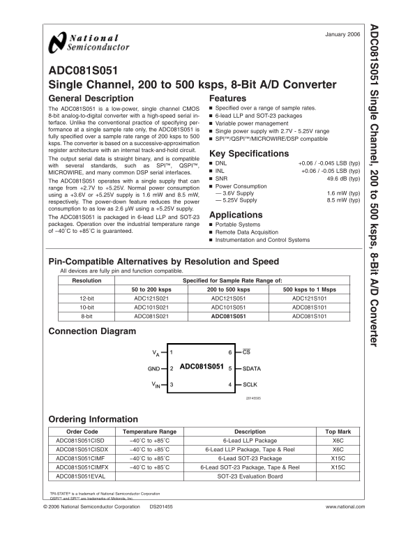
Page 1 Text Content
January
081S ingle hannel,200 to ksps,8-B it /D onverter
ADC081S051 Single Channel, to ksps, 8-Bit A/D Converter General Description Features
The ADC081S051 is low-power, single channel CMOS Specified over range of sample rates. 8-bit analog-to-digital converter with high-speed serial in- 6-lead LLP and SOT-23 packages
terface. Unlike the conventional practice of specifying per- Variable power management formance at single sample rate only, the ADC081S051 is
Single power supply with 2.7V 5.25V range
fully specified over sample rate range of ksps to
SPI™/QSPI™/MICROWIRE/DSP compatible
ksps. The converter is based on successive-approximation register architecture with an internal track-and-hold circuit.
Key Specifications
The output serial data is straight binary, and is compatible
DNL +0.06 -0.045 LSB (typ)
with several standards, such as SPI™, QSPI™,
INL +0.06 -0.05 LSB (typ)
MICROWIRE, and many common DSP serial interfaces.
SNR 49.6 d B (typ)
The ADC081S051 operates with single supply that can
Power Consumption
range from +2.7V to +5.25V. Normal power consumption
3.6V Supply 1.6 m W (typ)
using +3.6V or +5.25V supply is 1.6 m W and 8.5 m W,
5.25V Supply 8.5 m W (typ)
respectively. The power-down feature reduces the power consumption to as low as 2.6 µW using +5.25V supply.
The ADC081S051 is packaged in 6-lead LLP and SOT-23 Applications
packages. Operation over the industrial temperature range Portable Systems of −40˚C to +85˚C is guaranteed. Remote Data Acquisition
Instrumentation and Control Systems
Pin-Compatible Alternatives by Resolution and Speed All devices are fully pin and function compatible. Resolution Specified for Sample Rate Range of:
to ksps to ksps ksps to Msps
12-bit ADC121S021 ADC121S051 ADC121S101 10-bit ADC101S021 ADC101S051 ADC081S101 8-bit ADC081S021 ADC081S051 ADC081S101
Connection Diagram
Ordering Information Order Code Temperature Range Description Mark ADC081S051CISD −40˚C to +85˚C 6-Lead LLP Package X6C ADC081S051CISDX −40˚C to +85˚C 6-Lead LLP Package, Tape Reel X6C ADC081S051CIMF −40˚C to +85˚C 6-Lead SOT-23 Package X15C ADC081S051CIMFX −40˚C to +85˚C 6-Lead SOT-23 Package, Tape Reel X15C ADC081S051EVAL SOT-23 Evaluation Board
TRI-STATE® is trademark of National Semiconductor Corporation QSPI™ and SPI™ are trademarks of Motorola, Inc.
National Semiconductor Corporation DS201455 www.national.com
Page Summary Contents For NATIONAL SEMICONDUCTOR - ADC081S051 Single Channel Data Sheet, 200 to 500 ksps, 8-Bit Analog-to-Digital Converter
Manual Details
| Brand | National |
|---|---|
| Pages | 17 |
| File Size | 732.67 KB |
| Published | June 18, 2026 |
Enter the captcha to get the download link:

Frequently Asked Questions
What is the operable sample rate range for this converter?
The ADC081S051 operates over a sample rate range of 200 ksps to 500 ksps.
What single supply voltage does the device support?
It supports a full single power supply from +2.7V up to +5.25V.
How is data output received by the system?
The output samples are clocked out of pin 5 SDATA on falling edges of the SCLK pin.
What is its operating temperature range?
It guarantees operation over the industrial temperature range of −40˚C to +85˚C.