# A B C D E F G H I J K L M N O P Q R S T U V W X Y Z

National Semiconductor DAC101C081/C085 10-Bit Micro Power Digital-to-Analog Converter Data Sheet Manual

Summary

The DAC101C081/DAC101C085 is a high-precision, 10-bit micro-power Digital-to-Analog Converter (DAC). This manual provides comprehensive details on its operation, featuring an I²C-compatible two-wire interface and extended supply range (2.7V to 5.5V) for maximum flexibility. Ideal for designers building low-power applications such as portable instruments, industrial process control systems, or test equipment that requires exceptional accuracy and minimal power consumption.
📄 Preview 📖 Table of Contents Contents PAGE OF 24

Page 1 Text Content

/ D -B it M ic ro r D ig ita l-to -A lo rte

March 13, 2008

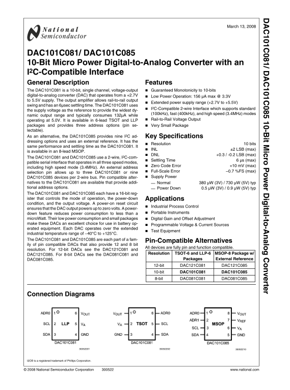
DAC101C081/ DAC101C085 10-Bit Micro Power Digital-to-Analog Converter with an I2C-Compatible Interface General Description Features The DAC101C081 is a 10-bit, single channel, voltage-output Guaranteed Monotonicity to 10-bits digital-to-analog converter (DAC) that operates from a +2.7V

Low Power Operation: 156 µA max @ 3.3V

to 5.5V supply. The output amplifier allows rail-to-rail output

Extended power supply range (+2.7V to +5.5V)

swing and has an 6µsec settling time. The DAC101C081 uses

I2C-Compatible 2-wire Interface which supports standard

the supply voltage as the reference to provide the widest dy-

(100k Hz), fast (400k Hz), and high speed (3.4MHz) modes

namic output range and typically consumes 132µA while

Rail-to-Rail Voltage Output

operating at 5.0V. It is available in 6-lead TSOT and LLP packages and provides three address options (pin se- Very Small Package lectable). As an alternative, the DAC101C085 provides nine I2C ad- Key Specifications dressing options and uses an external reference. It has the

Resolution 10 bits

same performance and settling time as the DAC101C081. It

INL ±2 LSB (max)

is available in an 8-lead MSOP.

DNL +0.3 / -0.2 LSB (max)

The DAC101C081 and DAC101C085 use a 2-wire, I2C-com-

Settling Time 6 µs (max)

patible serial interface that operates in all three speed modes,

Zero Code Error +10 m V (max)

including high speed mode (3.4MHz). An external address

Full-Scale Error −0.7 %FS (max)

selection pin allows up to three DAC101C081 or nine

DAC101C085 devices per 2-wire bus. Pin compatible alter- Supply Power

natives to the DAC101C081 are available that provide addi- Normal 380 µW (3V) / 730 µW (5V) typ tional address options. Power Down 0.5 µW (3V) / 0.9 µW (5V) typ The DAC101C081 and DAC101C085 each have a 16-bit reg- ister that controls the mode of operation, the power-down Applications condition, and the output voltage. A power-on reset circuit

Industrial Process Control

ensures that the DAC output powers up to zero volts. A power-

down feature reduces power consumption to less than a Portable Instruments

micro Watt. Their low power consumption and small packages Digital Gain and Offset Adjustment make these DACs an excellent choice for use in battery op-

Programmable Voltage & Current Sources

erated equipment. Each DAC operates over the extended

Test Equipment

industrial temperature range of −40°C to +125°C. The DAC101C081 and DAC101C085 are each part of a fam-

Pin-Compatible Alternatives

ily of pin compatible DACs that also provide 12 and 8 bit

All devices are fully pin and function compatible.

resolution. For 12-bit DACs see the DAC121C081 and

Resolution TSOT-6 and LLP-6 MSOP-8 Package w/

DAC121C085. For 8-bit DACs see the DAC081C081 and

DAC081C085. Packages External Reference

12-bit DAC121C081 DAC121C085 10-bit DAC101C081 DAC101C085 8-bit DAC081C081 DAC081C085

Connection Diagrams

I2C® is a registered trademark of Phillips Corporation.

© 2008 National Semiconductor Corporation www.national.com

Page Summary Contents For National Semiconductor DAC101C081/C085 10-Bit Micro Power Digital-to-Analog Converter Data Sheet Manual

Page 1 / D -B it M ic ro r D ig ita l-to -A lo rte March 13, 2008 DAC101C081/ DAC101C085 10-Bit Micro Power Digital-to-Analog Converter with an I2C-Compatible Interface General Description Features The DAC10...
Page 2 Ordering Information Order Code Temperature Range Package Top Mark DAC101C081CIMK −40°C ≤ TA ≤ +125°C TSOT X85C DAC101C081CIMKX −40°C ≤ TA ≤ +125°C TSOT Tape-and-Reel X85C DAC101C081CISD −40°C ≤ TA ≤ ...
Page 3 Pin Descriptions Symbol Type Equivalent Circuit Description VOUT Analog Output Analog Output Voltage. Power supply input. For the TSOT and LLP versions, this VA Supply supply is used as the reference....
Page 4 Absolute Maximum Ratings Operating Ratings (Notes 1, 2) (Notes 1, 2) Operating Temperature Range −40°C ≤ TA ≤ +125°C If Military/Aerospace specified devices are required, Supply Voltage, VA +2.7V to 5...
Page 5 Typical Limits Units Symbol Parameter Conditions (Note 9) (Note 9) (Limits) Output Short Circuit Current VA = 3V, VOUT = 3V, Input Code = 000h. −52 m A IOS (ISINK) VA = 5V, VOUT = 5V, Input Code = 000...
Page 6 Typical Limits Units Symbol Parameter Conditions (Note 9) (Note 9) (Limits) POWER REQUIREMENTS Supply Voltage Minimum 2.7 V (min) VA Supply Voltage Maximum 5.5 V (max) Normal -- VOUT set to midscale. ...
Page 7 A.C. and Timing Characteristics Values shown in this table are design targets and are subject to change before product release. The following specifications apply for VA = +2.7V to +5.5V, VREF = VA, R...
Page 8 Limits Typical Units Symbol Parameter Conditions (Note 13) (Notes 9, (Note 9) (Limits) Standard Mode ns (max) 20+0.1Cb ns (min) Fast Mode ns (max) tr DA Rise time of SDA signal ns (min) High Speed Mod...
Page 9 Note 6: Reflow temperature profiles are different for lead-free packages. / D Note 7: The inputs are protected as shown below. Input voltage magnitudes up to 5.5V, regardless of VA, will not cause err...
Page 10 Transfer Characteristic FIGURE 1. Input / Output Transfer Characteristic Timing Diagrams FIGURE 2. Serial Timing Diagram www.national.com
Page 11 Typical Performance Characteristics VREF = VA, f SCL = 3.4MHz, TA = 25°C, Input Code Range 12 to 1011, unless otherwise stated. INL DNL INL/DNL vs Temperature at VA = 3.0V INL/DNL vs Temperature at VA...
Page 12 INL/DNL vs VA Zero Code Error vs. VA Zero Code Error vs. Temperature Full Scale Error vs. VA Full Scale Error vs. Temperature Total Supply Current vs. VA www.national.com
Page 13 / D VREF Supply Current vs. VA Total Supply Current vs. Temperature @ VA = 3V Total Supply Current vs. Temperature @ VA = 5V 5V Glitch Response Power-On Reset www.national.com
Page 14 1.0 Functional Description 1.1 DAC SECTION 1.2 OUTPUT AMPLIFIER The DAC101C081 is fabricated on a CMOS process with an The output amplifier is rail-to-rail, providing an output voltage architecture th...
Page 15 1.4 SERIAL INTERFACE / D master is writing data, the slave ACKs after every data byte The I2C-compatible interface operates in all three speed is successfully received. When the master is reading data...
Page 16 1.4.3 High-Speed (Hs) Mode address to the DAC101C081, and communication continues For Hs-mode, the sequence of events to begin communica- as shown above in the "Basic Operation" Diagram (see...
Page 17 1.4.5 Writing to the DAC Register / D either sends the upper byte of the next data word to be con- To write to the DAC, the master addresses the part with the verted by the DAC, generates a Stop condi...
Page 18 1.5 DAC REGISTER 1.8 POWER-DOWN MODES The DAC register, Figure 8, has sixteen bits. The first two bits The DAC101C081 has three power-down modes. In power- are always zero. The next two bits determine...
Page 19 / D 2.1.2 LM4050 2.0 Applications Information Available with accuracy of 0.44%, the LM4050 shunt refer- 2.1 USING REFERENCES AS POWER SUPPLIES ence is also a good choice as a reference for the DAC101C...
Page 20 2.1.3 LP3985 2.2 BIPOLAR OPERATION The LP3985 is a low noise, ultra low dropout voltage regulator The DAC101C081 is designed for single supply operation and with a 3% accuracy over temperature. It is ...
Page 21 2.3 DSP/MICROPROCESSOR INTERFACING / D 2.3.2 Interfacing to a Hs-mode Bus Interfacing the DAC101C081 to microprocessors and DSPs Interfacing to a Hs-mode bus is very similar to interfacing to is quite...
Page 22 Physical Dimensions inches (millimeters) unless otherwise noted 6-Lead TSOT Order Numbers DAC101C081CIMK NS Package Number MK06A 6-Lead LLP Order Numbers DAC101C081CISD NS Package Number SDB06A www.na...
Page 23 8-Lead MSOP Order Numbers DAC101C085CIMM NS Package Number MUA08A www.national.com
Page 24 -B it ic ro ig it l- to -A lo rt Notes For more National Semiconductor product information and proven design tools, visit the following Web sites at: Products Design Support Amplifiers www.national.co...

Manual Details

Brand National
Pages 24
File Size 644.97 KB
Published June 05, 2026
55 views

Enter the captcha to get the download link:

captcha

Frequently Asked Questions

How many devices can share the same I²C bus?

It supports up to three DAC101C081 or nine DAC101C085 devices per 2-wire bus using external address selection.

What is the operating voltage range for this converter?

The DAC operates over an extended supply voltage range of +2.7V to +5.5V, allowing rail-to-rail output.

Does it offer low power consumption modes?

Yes, the device features a Power Down function that reduces power consumption to less than one microWatt, ideal for battery operation.