National Semiconductor DAC0800 DAC0802 8-Bit Digital-to-Analog Converter User Manual
Summary
These high-performance DAC0800 and DAC0802 series are monolithic 8-bit Digital-to-Analog Converters designed for robust signal processing in general electronics. The manual provides comprehensive technical specifications covering rapid settling times (100 ns), bipolar output capabilities (-10V to +18V), wide supply voltage ranges, and low power consumption. Essential for engineers requiring precise, high-speed data conversion with minimal nonlinearity.
Page 1 Text Content
查询DAC0800供应商
0800/D 8-B it igital-to-A nalog onverters
DAC0800/DAC0802 8-Bit Digital-to-Analog Converters
The DAC0800, DAC0802, DAC0800C and DAC0802C are
General Description
direct replacement for the DAC-08, DAC-08A, DAC-08C,
The DAC0800 series are monolithic 8-bit high-speed
and DAC-08H, respectively.
current-output digital-to-analog converters (DAC) featuring typical settling times of ns. When used as multiplying
Features
DAC, monotonic performance over to reference cur-
rent range is possible. The DAC0800 series also features Fast settling output current: ns
high compliance complementary current outputs to allow dif- Full scale error: ±1 LSB
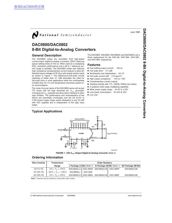
ferential output voltages of Vp-p with simple resistor loads Nonlinearity over temperature: ±0.1% as shown in Figure 1. The reference-to-full-scale current Full scale current drift: ±10 ppm/˚C
matching of better than ±1 LSB eliminates the need for
High output compliance: −10V to +18V
full-scale trims in most applications while the nonlinearities
Complementary current outputs
of better than ±0.1% over temperature minimizes system er-
Interface directly with TTL, CMOS, PMOS and others
ror accumulations.
quadrant wide range multiplying capability
The noise immune inputs of the DAC0800 series will accept
Wide power supply range: ±4.5V to ±18V
TTL levels with the logic threshold pin, VLC, grounded.
Low power consumption: m W at ±5V
Changing the VLC potential will allow direct interface to other
logic families. The performance and characteristics of the Low cost
device are essentially unchanged over the full ±4.5V to
±18V power supply range; power dissipation is only m W with ±5V supplies and is independent of the logic input states.
Typical Applications
DS005686-1
FIGURE 1. ±20 VP-P Output Digital-to-Analog Converter (Note 5)
Ordering Information Non-Linearity Temperature Order Numbers
Range Package (J16A) (Note 1) Package (N16E) (Note 1) SO Package (M16A)
±0.1% FS 0˚C TA +70˚C DAC0802LCJ DAC-08HQ DAC0802LCN DAC-08HP DAC0802LCM ±0.19% FS −55˚C TA +125˚C DAC0800LJ DAC-08Q ±0.19% FS 0˚C TA +70˚C DAC0800LCJ DAC-08EQ DAC0800LCN DAC-08EP DAC0800LCM Note 1: Devices may be ordered by using either order number.
National Semiconductor Corporation DS005686 www.national.com
Page Summary Contents For National Semiconductor DAC0800 DAC0802 8-Bit Digital-to-Analog Converter User Manual
Manual Details
| Brand | National |
|---|---|
| Pages | 11 |
| File Size | 346.48 KB |
| Published | June 15, 2026 |
Enter the captcha to get the download link:
