# A B C D E F G H I J K L M N O P Q R S T U V W X Y Z

National Semiconductor - ADC124S021 4 Channel, 50ksps to 200ksps, 12-Bit AD Converter Owner's Manual

Summary

This low-power, four-channel 12-bit ADC converts analog signals into high-speed digital data across a sample rate range of 50 ksps to 200 ksps. Designed for applications in portable systems, remote data acquisition, and control instrumentation, it operates on a stable single supply (2.7V to 5.25V). The manual provides comprehensive details on its high-speed serial interface compatibility (SPI/QSPI), meticulous specifications like INL and DNL, power consumption features, and full operational characteristics for reliable integration into complex systems.
📄 Preview 📖 Table of Contents Contents PAGE OF 20

Page 1 Text Content

l, 5 to , 1 -B it A /D rte

August 4, 2008

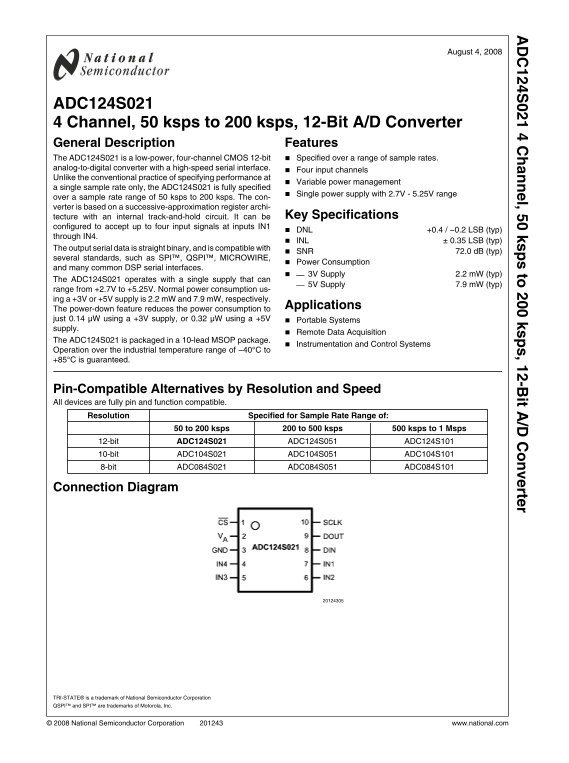
ADC124S021 4 Channel, 50 ksps to 200 ksps, 12-Bit A/D Converter General Description Features The ADC124S021 is a low-power, four-channel CMOS 12-bit Specified over a range of sample rates. analog-to-digital converter with a high-speed serial interface.

Four input channels

Unlike the conventional practice of specifying performance at

Variable power management

a single sample rate only, the ADC124S021 is fully specified

Single power supply with 2.7V - 5.25V range

over a sample rate range of 50 ksps to 200 ksps. The con- verter is based on a successive-approximation register archi-

tecture with an internal track-and-hold circuit. It can be Key Specifications

configured to accept up to four input signals at inputs IN1

DNL +0.4 / −0.2 LSB (typ)

through IN4.

INL ± 0.35 LSB (typ)

The output serial data is straight binary, and is compatible with

SNR 72.0 d B (typ)

several standards, such as SPI™, QSPI™, MICROWIRE,

Power Consumption

and many common DSP serial interfaces.

3V Supply 2.2 m W (typ)

The ADC124S021 operates with a single supply that can

5V Supply 7.9 m W (typ)

range from +2.7V to +5.25V. Normal power consumption us- ing a +3V or +5V supply is 2.2 m W and 7.9 m W, respectively.

Applications

The power-down feature reduces the power consumption to just 0.14 µW using a +3V supply, or 0.32 µW using a +5V Portable Systems supply.

Remote Data Acquisition

The ADC124S021 is packaged in a 10-lead MSOP package.

Instrumentation and Control Systems

Operation over the industrial temperature range of −40°C to +85°C is guaranteed.

Pin-Compatible Alternatives by Resolution and Speed All devices are fully pin and function compatible. Resolution Specified for Sample Rate Range of:

50 to 200 ksps 200 to 500 ksps 500 ksps to 1 Msps 12-bit ADC124S021 ADC124S051 ADC124S101 10-bit ADC104S021 ADC104S051 ADC104S101 8-bit ADC084S021 ADC084S051 ADC084S101

Connection Diagram

TRI-STATE® is a trademark of National Semiconductor Corporation QSPI™ and SPI™ are trademarks of Motorola, Inc.

© 2008 National Semiconductor Corporation www.national.com

Page Summary Contents For National Semiconductor - ADC124S021 4 Channel, 50ksps to 200ksps, 12-Bit AD Converter Owner's Manual

Page 1 l, 5 to , 1 -B it A /D rte August 4, 2008 ADC124S021 4 Channel, 50 ksps to 200 ksps, 12-Bit A/D Converter General Description Features The ADC124S021 is a low-power, four-channel CMOS 12-bit Specified...
Page 2 Ordering Information Order Code Temperature Range Description Top Mark ADC124S021CIMM −40°C to +85°C 10-Lead MSOP Package X21C ADC124S021CIMMX −40°C to +85°C 10-Lead MSOP Package, Tape & Reel X21C...
Page 3 Absolute Maximum Ratings (Notes 1, 2) Operating Ratings (Notes 1, 2) Operating Temperature Range −40°C ≤ TA ≤ +85°C If Military/Aerospace specified devices are required, please contact the National Se...
Page 4 Limits Symbol Parameter Conditions Typical Units (Note 7) ANALOG INPUT CHARACTERISTICS VIN Input Range 0 to VA IDCL DC Leakage Current ±0.02 ±1 µA (max) Track Mode p F CINA Input Capacitance Hold Mode...
Page 5 ADC124S021 Timing Specifications The following specifications apply for VA = +2.7V to 5.25V, GND = 0V, f SCLK = 0.8 MHz to 3.2 MHz, f SAMPLE = 50 ksps to 200 ksps, CL = 35 p F, Boldface limits apply f...
Page 6 Timing Diagrams ADC124S021 Operational Timing Diagram Timing Test Circuit ADC124S021 Serial Timing Diagram SCLK and CS Timing Parameters www.national.com
Page 7 INTERMODULATION DISTORTION (IMD) is the creation of Specification Definitions additional spectral components as a result of two sinusoidal ACQUISITION TIME is the time required to acquire the input fr...
Page 8 Typical Performance Characteristics TA = +25°C, f SAMPLE = 50 ksps to 200 ksps, f SCLK = 0.8 MHz to 3.2 MHz, f IN = 39.9 k Hz unless otherwise stated. DNL - VA = 3.0V INL - VA = 3.0V DNL - VA = 5.0V I...
Page 9 DNL vs. Clock Frequency INL vs. Clock Frequency DNL vs. Clock Duty Cycle INL vs. Clock Duty Cycle DNL vs. Temperature INL vs. Temperature www.national.com
Page 10 SNR vs. Supply THD vs. Supply SNR vs. Clock Frequency THD vs. Clock Frequency SNR vs. Clock Duty Cycle THD vs. Clock Duty Cycle www.national.com
Page 11 SNR vs. Input Frequency THD vs. Input Frequency SNR vs. Temperature THD vs. Temperature SFDR vs. Supply SINAD vs. Supply www.national.com
Page 12 SFDR vs. Clock Frequency SINAD vs. Clock Frequency SFDR vs. Clock Duty Cycle SINAD vs. Clock Duty Cycle SFDR vs. Input Frequency SINAD vs. Input Frequency www.national.com
Page 13 SFDR vs. Temperature SINAD vs. Temperature ENOB vs. Supply ENOB vs. Clock Frequency ENOB vs. Clock Duty Cycle ENOB vs. Input Frequency www.national.com
Page 14 ENOB vs. Temperature Spectral Response - 3V, 200 ksps Spectral Response - 5V, 200 ksps Power Consumption vs. Throughput www.national.com
Page 15 sampled voltage, and switch SW2 unbalances the compara- Applications Information tor. The control logic then instructs the charge-redistribution DAC to add fixed amounts of charge to the sampling capa...
Page 16 input that is selected for the conversion after the current one. There are no power-up delays or dummy conversions re- See Tables 1, 2 and 3. quired with the ADC124S021. The ADC is able to sample and ...
Page 17 FIGURE 4. Typical Application Circuit 5.0 ANALOG INPUTS mode between the 16th falling edge of a conversion and the An equivalent circuit for one of the ADC124S021's input chan- 1st falling edge of the...
Page 18 strate that will degrade noise performance if that current is greater than 35 p F, use a 100 Ω series resistor at the ADC large enough. The larger is the output capacitance, the more output, located a...
Page 19 Physical Dimensions inches (millimeters) unless otherwise noted 10-Lead MSOP Order Number ADC124S021CIMM, ADC124S021CIMMX NS Package Number P0MUB10A www.national.com
Page 20 l, -B it /D rt Notes For more National Semiconductor product information and proven design tools, visit the following Web sites at: Products Design Support Amplifiers www.national.com/amplifiers WEBEN...

Manual Details

Brand National
Pages 20
File Size 429.83 KB
Published June 18, 2026
5 views

Enter the captcha to get the download link:

captcha

Frequently Asked Questions

What is the operating voltage range for the ADC124S021?

It operates with a single supply ranging from +2.7V to +5.25V.

How much power does the device consume at 3V and 5V supplies?

The normal power consumption is 2.2 mW using a +3V supply, and 7.9 mW using a +5V supply.

What are the supported programming/serial interfaces for data output?

It is compatible with several standards, including SPI™, QSPI™, MICROWIRE, and many common DSP serial interfaces.

Can this device be used in industrial temperature environments?

Yes, operation over the industrial range of −40°C to +85°C is guaranteed.