National Semiconductor CD4051BM BC CD4051B Single-channel 8 Analog Data Manual
Summary
Engineered for precise signal routing in analog systems, these multiplexers and demultiplexers allow designers to digitally control analog signals up to 15V p-p. The series offers scalable switching capabilities—from single 8-channel to triple 2-channel setups—while featuring extremely low 'ON' resistance and minimal power dissipation. This manual provides comprehensive technical specifications, including detailed electrical characteristics, operating voltage ranges, and connection diagrams. Ideal for electronics engineers and circuit developers requiring reliable, high-performance signal multiplexing with integrated binary address decoding.
Page 1 Text Content
查询CD4051BCJ供应商
October
lo ltip le r/ ltip le rs CD4051BM/CD4051BC Single 8-Channel Analog Multiplexer/Demultiplexer CD4052BM/CD4052BC Dual 4-Channel Analog Multiplexer/Demultiplexer CD4053BM/CD4053BC Triple 2-Channel Analog Multiplexer/Demultiplexer General Description
These analog multiplexers/demultiplexers are digitally con- an inhibit input. Each control input selects one of pair of trolled analog switches having low ‘‘ON’’ impedance and channels which are connected in single-pole double-throw very low ‘‘OFF’’ leakage currents. Control of analog signals configuration.
up to 15Vp-p can be achieved by digital signal amplitudes of 3–15V. For example, if VDDe5V, VSSe0V and VEEeb5V, Features
analog signals from b5V to a5V can be controlled by digi-
Wide range of digital and analog signal levels: digital
tal inputs of 0–5V. The multiplexer circuits dissipate ex-
3–15V, analog to 15Vp-p
tremely low quiescent power over the full VDDb VSS and
Low ‘‘ON’’ resistance: 80X (typ.) over entire 15Vp-p sig-
VDDb VEE supply voltage ranges, independent of the logic
nal-input range for VDDb VEEe15V
state of the control signals. When logical ‘‘1’’ is present at
High ‘‘OFF’’ resistance: channel leakage of g10 p A
the inhibit input terminal all channels are ‘‘OFF’’.
(typ.) at VDDb VEEe10V
CD4051BM/CD4051BC is single 8-channel multiplexer
Logic level conversion for digital addressing signals of
having three binary control inputs. A, B, and C, and an inhibit
3–15V (VDDb VSSe3–15V) to switch analog signals to
input. The three binary signals select of channels to be
Vp-p (VDDb VEEe15V)
turned ‘‘ON’’ and connect the input to the output.
Matched switch characteristics: DRONe5X (typ.) for
CD4052BM/CD4052BC is differential 4-channel multiplex-
VDDb VEEe15V
er having two binary control inputs, and B, and an inhibit
Very low quiescent power dissipation under all digital-
input. The two binary input signals select or pairs of
control input and supply conditions: m W (typ.) at
channels to be turned on and connect the differential ana-
VDDb VSSe VDDb VEEe10V
log inputs to the differential outputs.
Binary address decoding on chip
CD4053BM/CD4053BC is triple 2-channel multiplexer having three separate digital control inputs, A, B, and C, and
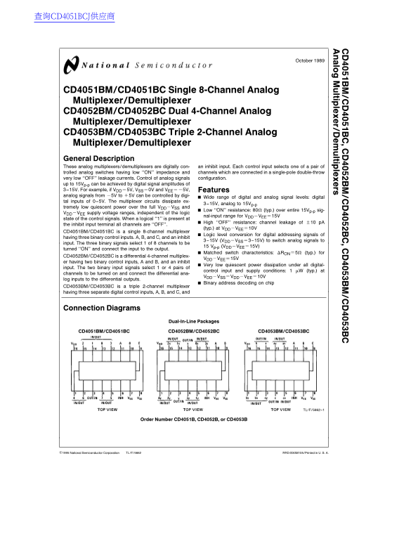
Connection Diagrams
Dual-In-Line Packages
CD4051BM/CD4051BC CD4052BM/CD4052BC CD4053BM/CD4053BC
TL/F/5662–1
Order Number CD4051B, CD4052B, or CD4053B
C1995 National Semiconductor Corporation TL/F/5662 RRD-B30M105/Printed in U. S. A.
Page Summary Contents For National Semiconductor CD4051BM BC CD4051B Single-channel 8 Analog Data Manual
Manual Details
| Brand | National |
|---|---|
| Pages | 10 |
| File Size | 190.70 KB |
| Published | June 16, 2026 |
Enter the captcha to get the download link:

Frequently Asked Questions
What is the maximum supply voltage range for the multiplexers?
The device operates at DC supply voltages between 5V and 15V.
How low are the 'OFF' channel leakage currents?
Channel leakage current is specified as low as 200 nA (CD4053) to 500 nA (CD4051) depending on the specific chip and voltage.
What differentiates the three models (4051, 4052, 4053)?
The 4051 is single/8-channel, the 4052 is differential/4-channel, and the 4053 is a triple/2-channel multiplexer.
What is the typical 'ON' resistance for these components?
The typical 'ON' resistance (R_ON) across any channel at standard operating conditions ranges between 120 Ω to 550 Ω.