# A B C D E F G H I J K L M N O P Q R S T U V W X Y Z

NATIONAL SEMICONDUCTOR - LMV841 Single LMV844 Quad CMOS Input Operational Amplifiers Data Manual, Owner's Guide

Summary

Engineered for resource-constrained designs, the LMV841/LMV844 Operational Amplifiers offer high performance in low-voltage, low-power applications. These integrated circuits feature CMOS inputs, rail-to-rail output, and wide supply ranges (2.7V to 12V), making them ideal for battery-powered instrumentation and portable electronics. Ideal for sensor interface, active filters, and signal buffering requiring compactness (SC70/TSSOP). This guide provides comprehensive technical data sheets, detailing electrical characteristics and performance metrics necessary for reliable system design across various temperature ranges.
📄 Preview 📖 Table of Contents Contents PAGE OF 18

Page 1 Text Content

in le / L In t, R IO , W id ly ra tio l A lifie rs

March 2007

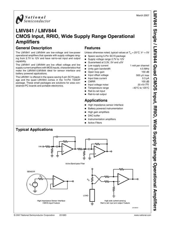
LMV841 / LMV844 CMOS Input, RRIO, Wide Supply Range Operational Amplifiers General Description Features The LMV841 and LMV844 are low-voltage and low-power Unless otherwise noted, typical values at TA = 25°C, V+ = 5V operational amplifiers that operate with supply voltages rang- Space saving 5-Pin SC70 package ing from 2.7V to 12V and have rail-to-rail input and output

Supply voltage range 2.7V to 12V

capability.

Guaranteed at 3.3V, 5V and ±5V

The LMV841 and LMV844 are low offset voltage and low

Low supply current 1 m A per channel

supply current amplifiers with MOS inputs, characteristics that

Unity gain bandwidth 4.5 MHz

make the LMV841/LMV844 ideal for sensor interface and

Open loop gain 100 d B

battery powered applications.

Input offset voltage 500 μV max

The LMV841 is offered in the space saving 5-pin SC70 pack-

Input bias current 0.3 p A

age and the quad LMV844 comes in the 14-Pin TSSOP

CMRR 100 d B

package. These small packages are solutions for area con-

Input voltage noise 20 n V/

strained PC boards and portable electronics.

Temperature range −40°C to 125°C Rail-to-rail input Rail-to-rail output

Applications High impedance sensor interface Battery powered instrumentation High gain amplifiers DAC buffer Instrumentation amplifiers Active Filters

Typical Applications

© 2007 National Semiconductor Corporation www.national.com

Page Summary Contents For NATIONAL SEMICONDUCTOR - LMV841 Single LMV844 Quad CMOS Input Operational Amplifiers Data Manual, Owner's Guide

Page 1 in le / L In t, R IO , W id ly ra tio l A lifie rs March 2007 LMV841 / LMV844 CMOS Input, RRIO, Wide Supply Range Operational Amplifiers General Description Features The LMV841 and LMV844 are low-volt...
Page 2 in le Junction Temperature (Note 3) +150°C Absolute Maximum Ratings (Note 1) Soldering Information If Military/Aerospace specified devices are required, Infrared or Convection (20 sec) 235°C please co...
Page 3 in le / L Symbol Parameter Conditions Min Typ Max Units (Note 6) (Note 5) (Note 6) en Input-Referred Voltage Noise f = 1 k Hz n V/ ROUT Open Loop Output Impedance f = 3 MHz THD+N Total Harmonic Distor...
Page 4 in le Symbol Parameter Conditions Min Typ Max Units (Note 6) (Note 5) (Note 6) THD+N Total Harmonic Distortion + Noise f = 1 k Hz , AV = 1 0.003 RL = 10 kΩ CIN Input Capacitance p F ±5V Electrical Cha...
Page 5 Note 1: Absolute Maximum Ratings indicate limits beyond which damage to the device may occur. Operating Ratings indicate conditions for which the device is in le / L intended to be functional, but spe...
Page 6 in le Typical Performance Characteristics At TA = 25°C, RL = 10 kΩ, VS = 5V. Unless otherwise specified. VOS vs. VCM Over Temperature at 3.3V VOS vs. VCM Over Temperature at 5.0V VOS vs. VCM Over Temp...
Page 7 in le / L Input Bias Current vs. VCM Input Bias Current vs. VCM Input Bias Current vs. VCM Supply Current vs. Supply Voltage Sinking Current vs. Supply Voltage Sourcing Current vs. Supply Voltage www....
Page 8 in le Output Swing High vs. Supply Voltage RL = 2k Output Swing High vs. Supply Voltage RL = 10k Output Swing Low vs. Supply Voltage RL = 2k Output Swing Low vs. Supply Voltage RL = 10k Output Voltage...
Page 9 in le / L Open Loop Frequency Response Over Load Conditions Phase Margin vs. CL PSRR vs. Frequency CMRR vs. Frequency Channel separation vs. Frequency Large Signal Step Response With GAIN = 1 www.nati...
Page 10 in le Large Signal Step Response With GAIN = 10 Small Signal Step Response With GAIN = 1 Small Signal Step Response With GAIN = 10 Overshoot vs CL Input Voltage Noise vs. Frequency THD+N vs. Frequency...
Page 11 in le / L THD+N vs. VOUT Closed Loop Output Impedance vs. Frequency www.national.com
Page 12 To reduce this small offset shift, the amplifier is trimmed dur- in le Application Information ing production, resulting in an input offset voltage of less then 0.5 m V at room temperature over the to...
Page 13 However, using low resistor values will increase the power in le / L a center frequency of approximately 10% from the frequency consumption of the application. This is not always acceptable of the tot...
Page 14 The filter responses of filter A and filter B are shown as the The voltage at the input of the op amp can be calculated by in le thin lines in Figure 4, the response of the combined filter is VIN+ = V...
Page 15 in le / L When we use 2 kΩ for RG, we can calculate the value for RF with this gain of 160. We can use AV = RF / RG to calculate the gain, so we can calculate RF by using RF = AV x RG = 160 x 2 kΩ = 3...
Page 16 in le Physical Dimensions inches (millimeters) unless otherwise noted 5-Pin SC70 NS Package Number MAA05A 14–Pin TSSOP NS Package Number MTC14 www.national.com
Page 17 in le / L Notes www.national.com
Page 18 in le t, IO id ly ra ti li fi rs Notes THE CONTENTS OF THIS DOCUMENT ARE PROVIDED IN CONNECTION WITH NATIONAL SEMICONDUCTOR CORPORATION (“NATIONAL”) PRODUCTS. NATIONAL MAKES NO REPRESENTATIONS OR WARR...