# A B C D E F G H I J K L M N O P Q R S T U V W X Y Z

AD7656 AD7657 AD7658 16-14-12-Bit Bipolar ADC User Manual Specifications

Summary

High-performance data acquisition is simplified with these six-channel, high-speed ADCs. These devices support simultaneous sampling of true bipolar signals up to 250 kSPS, making them ideal for complex monitoring and control systems. This resource manual provides a comprehensive guide covering functional block diagrams, operational theory, key features (including parallel and serial interfaces), power specifications, and diverse applications in instrumentation and power line monitoring. It is designed for engineers developing professional data processing equipment.
📄 Preview 📖 Table of Contents Contents PAGE OF 32

Page 1 Text Content

250 k SPS, 6-Channel, Simultaneous Sampling, Bipolar 16-/14-/12-Bit ADC

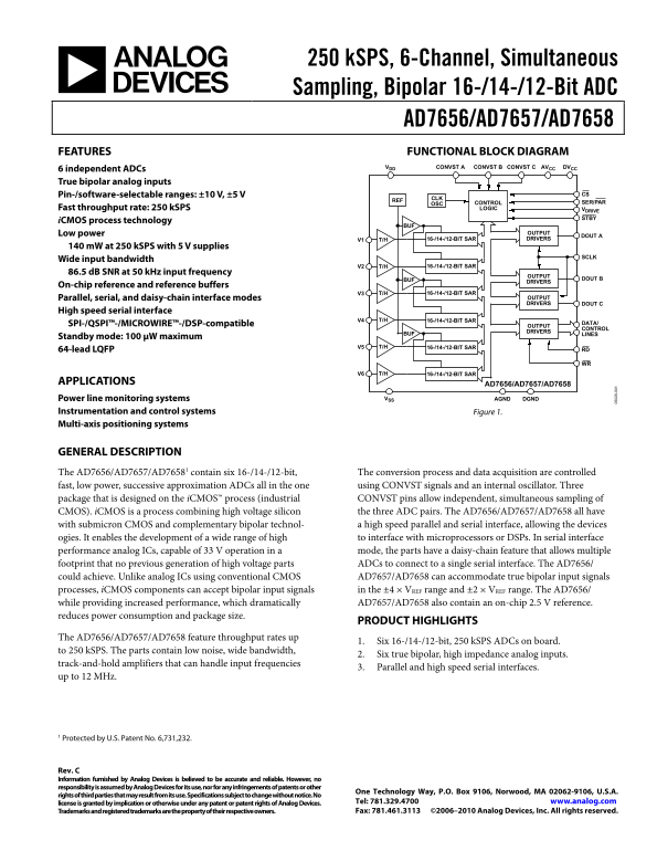
AD7656/AD7657/AD7658 FEATURES FUNCTIONAL BLOCK DIAGRAM

VDD CONVST A CONVST B CONVST C AVCC DVCC

6 independent ADCs True bipolar analog inputs

Pin-/software-selectable ranges: ±10 V, ±5 V CS

REF CLK

OSC CONTROL SER/PAR

Fast throughput rate: 250 k SPS LOGIC VDRIVE

i CMOS process technology

Low power OUTPUT

DOUT A

V1 T/H 16-/14-/12-BIT SAR DRIVERS

140 m W at 250 k SPS with 5 V supplies

Wide input bandwidth

V2 T/H 16-/14-/12-BIT SAR

86.5 d B SNR at 50 k Hz input frequency

OUTPUT

BUF DOUT B

DRIVERS

On-chip reference and reference buffers

V3 T/H 16-/14-/12-BIT SAR

Parallel, serial, and daisy-chain interface modes OUTPUT DRIVERS DOUT C

High speed serial interface

V4 T/H 16-/14-/12-BIT SAR

SPI-/QSPI™-/MICROWIRE™-/DSP-compatible DATA/

OUTPUT

CONTROL

BUF DRIVERS

LINES

Standby mode: 100 μW maximum

V5 T/H 16-/14-/12-BIT SAR

64-lead LQFP RD WR

V6 T/H 16-/14-/12-BIT SAR

APPLICATIONS

Power line monitoring systems VSS AGND DGND

Instrumentation and control systems Figure 1. Multi-axis positioning systems

GENERAL DESCRIPTION

The AD7656/AD7657/AD76581 contain six 16-/14-/12-bit, The conversion process and data acquisition are controlled fast, low power, successive approximation ADCs all in the one using CONVST signals and an internal oscillator. Three package that is designed on the i CMOS™ process (industrial CONVST pins allow independent, simultaneous sampling of CMOS). i CMOS is a process combining high voltage silicon the three ADC pairs. The AD7656/AD7657/AD7658 all have with submicron CMOS and complementary bipolar technol- a high speed parallel and serial interface, allowing the devices ogies. It enables the development of a wide range of high to interface with microprocessors or DSPs. In serial interface performance analog ICs, capable of 33 V operation in a mode, the parts have a daisy-chain feature that allows multiple footprint that no previous generation of high voltage parts ADCs to connect to a single serial interface. The AD7656/ could achieve. Unlike analog ICs using conventional CMOS AD7657/AD7658 can accommodate true bipolar input signals processes, i CMOS components can accept bipolar input signals in the ±4 × VREF range and ±2 × VREF range. The AD7656/ while providing increased performance, which dramatically AD7657/AD7658 also contain an on-chip 2.5 V reference.

reduces power consumption and package size. 0- 1AD7656/AD7657/AD7658

PRODUCT HIGHLIGHTS

The AD7656/AD7657/AD7658 feature throughput rates up

1. Six 16-/14-/12-bit, 250 k SPS ADCs on board.

to 250 k SPS. The parts contain low noise, wide bandwidth,

2. Six true bipolar, high impedance analog inputs.

track-and-hold amplifiers that can handle input frequencies

3. Parallel and high speed serial interfaces.

up to 12 MHz.

1 Protected by U.S. Patent No. 6,731,232.

Rev. C Information furnished by Analog Devices is believed to be accurate and reliable. However, no responsibility is assumed by Analog Devices for its use, nor for any infringements of patents or other

One Technology Way, P.O. Box 9106, Norwood, MA 02062-9106, U.S.A.

rights of third parties that may result from its use. Specifications subject to change without notice. No

license is granted by implication or otherwise under any patent or patent rights of Analog Devices. Tel: 781.329.4700 www.analog.com Trademarks and registered trademarks are the property of their respective owners. Fax: 781.461.3113 ©2006–2010 Analog Devices, Inc. All rights reserved.

Page Summary Contents For AD7656 AD7657 AD7658 16-14-12-Bit Bipolar ADC User Manual Specifications

Page 1 250 k SPS, 6-Channel, Simultaneous Sampling, Bipolar 16-/14-/12-Bit ADC AD7656/AD7657/AD7658 FEATURES FUNCTIONAL BLOCK DIAGRAM VDD CONVST A CONVST B CONVST C AVCC DVCC 6 independent ADCs True bipolar ...
Page 2 AD7656/AD7657/AD7658 TABLE OF CONTENTS Features .............................................................................................. 1 Typical Performance Characteristics ......................
Page 3 AD7656/AD7657/AD7658 SPECIFICATIONS AD7656 VREF = 2.5 V internal/external, AVCC = 4.75 V to 5.25 V, DVCC = 4.75 V to 5.25 V, VDRIVE = 2.7 V to 5.25 V; For ±4 × VREF range: VDD = 10 V to 16.5 V, VSS = ...
Page 4 AD7656/AD7657/AD7658 Parameter B Version1 Y Version1 Unit Test Conditions/Comments LOGIC INPUTS Input High Voltage (VINH) 0.7 × VDRIVE 0.7 × VDRIVE V min Input Low Voltage (VINL) 0.3 × VDRIVE 0.3 × VD...
Page 5 AD7656/AD7657/AD7658 AD7657 VREF = 2.5 V internal/external, AVCC = 4.75 V to 5.25 V, DVCC = 4.75 V to 5.25 V, VDRIVE = 2.7 V to 5.25 V; For ±4 × VREF range: VDD = 10 V to 16.5 V, VSS = −10 V to −16.5 ...
Page 6 AD7656/AD7657/AD7658 Parameter B Version1 Y Version1 Unit Test Conditions/Comments LOGIC OUTPUTS Output High Voltage (VOH) VDRIVE − 0.2 VDRIVE − 0.2 V min ISOURCE = 200 μA Output Low Voltage (VOL) 0.2...
Page 7 AD7656/AD7657/AD7658 AD7658 VREF = 2.5 V internal/external, AVCC = 4.75 V to 5.25 V, DVCC = 4.75 V to 5.25 V, VDRIVE = 2.7 V to 5.25 V; For ±4 × VREF range: VDD = 10 V to 16.5 V, VSS = −10 V to −16.5 ...
Page 8 AD7656/AD7657/AD7658 Parameter B Version1 Y Version1 Unit Test Conditions/Comments LOGIC OUTPUTS Output High Voltage (VOH) VDRIVE − 0.2 VDRIVE − 0.2 V min ISOURCE = 200 μA Output Low Voltage (VOL) 0.2...
Page 9 AD7656/AD7657/AD7658 TIMING SPECIFICATIONS AVCC/DVCC = 4.75 V to 5.25 V, VDD = 5 V to 16.5 V, VSS = −5 V to −16.5 V, VDRIVE = 2.7 V to 5.25 V, VREF = 2.5 V internal/external, TA = TMIN to TMAX, unless...
Page 10 AD7656/AD7657/AD7658 ABSOLUTE MAXIMUM RATINGS TA = 25°C, unless otherwise noted. Stresses above those listed under Absolute Maximum Ratings Table 5. may cause permanent damage to the device. This is a...
Page 11 AD7656/AD7657/AD7658 PIN CONFIGURATION AND FUNCTION DESCRIPTIONS 1DB14/REFBUFEN/DIS V6 PIN 1 2DB13 AVCC 3DB12 AVCC 4DB11 V5 5DB10/DOUT C AGND 6DB9/DOUT B AGND AD7656/AD7657/AD7658 7DB8/DOUT A V4 TOP V...
Page 12 AD7656/AD7657/AD7658 Pin No. Mnemonic Description 19 CS Chip Select. This active low logic input frames the data transfer. When both CS and RD are logic low in parallel mode, the output bus is enabled...
Page 13 AD7656/AD7657/AD7658 Pin No. Mnemonic Description 7 DB8/DOUT A Data Bit 8/Serial Data Output A. When SER/PAR = 0, this pin acts as a three-state parallel digital output pin. When SER/PAR = 1 and SEL A...
Page 14 IN (L SB (d (d AD7656/AD7657/AD7658 TYPICAL PERFORMANCE CHARACTERISTICS VDD/VSS = ±15V AVCC/DVCC/VDRIVE = +5V INTERNAL REFERENCE ±10V RANGE –40 TA = 25°C 1.0 f S = 250k SPS f IN = 50k Hz –60 SNR = +87...
Page 15 AD7656/AD7657/AD7658 SI (d (L SB IN (L SB f SAMPLE = 250k SPS 0.8 AVCC/DVCC/VDRIVE = +5V INTERNAL REFERENCE VDD/VSS = ±12V TA = 25°C –70 AVCC/DVCC/VDRIVE = +5V 0.6 f SAMPLE = 250k SPS VDD/VSS = ±5.25V...
Page 16 ER EN ES VE SI IM (µ s) EF ER EN VO LT (V AD7656/AD7657/AD7658 2.510 AVCC/DVCC/VDRIVE = +5V f SAMPLE = 250k SPS VDD/VSS = ±12V ±2 × VREF RANGE INTERNAL REFERENCE TA = 25°C 2.506 f IN = 10k Hz 100n F O...
Page 17 AD7656/AD7657/AD7658 EL -T EL IS LA TI (d ±10V RANGE ±5V RANGE AVCC/DVCC/VDRIVE = 5V VDD/VSS = ±12V TA = 25°C AVCC/DVCC/VDRIVE = +5V INTERNAL REFERENCE f SAMPLE = 250k SPS ±2 × VREF RANGE FOR ±5V RANG...
Page 18 AD7656/AD7657/AD7658 TERMINOLOGY The ratio depends on the number of quantization levels in the Integral Nonlinearity digitization process: the more levels, the smaller the quantization The maximum dev...
Page 19 AD7656/AD7657/AD7658 Figure 19 shows the power supply rejection ratio vs. supply Channel-to-Channel Isolation ripple frequency for the AD7656/AD7657/AD7658. Channel-to-channel isolation is a measure o...
Page 20 AD7656/AD7657/AD7658 THEORY OF OPERATION CONVERTER DETAILS Analog Input Section The AD7656/AD7657/AD7658 are high speed, low power The AD7656/AD7657/AD7658 can handle true bipolar input converters tha...
Page 21 AD7656/AD7657/AD7658 ADC TRANSFER FUNCTION the internal reference buffers can be disabled in hardware mode by setting the DB14/REFBUFEN/DIS pin high. If the The output coding of the AD7656/AD7657/AD76...
Page 22 AD7656/AD7657/AD7658 DIGITAL SUPPLY VOLTAGE +3V OR +5VANALOG SUPPLY VOLTAGE 5V1 100n F DVCCAVCCAGND DGND VDRIVE DGND +9.5V TO +16.5V SUPPLY 100n F 10µF PARALLEL DB0 TO DB15 AGND INTERFACE µP/µC/DSP CO...
Page 23 AD7656/AD7657/AD7658 The CS signal can be permanently tied low, and the RD signal can affect the performance of the conversion. For the specified can be used to access the conversion results. A read o...
Page 24 AD7656/AD7657/AD7658 Software Selection of ADCs Table 11. The H/S SEL pin determines the source of the combination of Bit Mnemonic Comment ADCs that are to be simultaneously sampled. When the H/S SEL ...
Page 25 AD7656/AD7657/AD7658 If it is required to clock conversion data out on two data out Changing the Analog Input Range (H/S SEL = 0) lines, DOUT A and DOUT B should be used. To enable DOUT A The AD7656/A...
Page 26 AD7656/AD7657/AD7658 CONVST A, CONVST B, CONVST C t ACQt CONVERT t QUIET DOUT A V1 V2 DOUT B V3 V4 DOUT C V5 V6 Figure 30. Serial Interface with Three DOUT Lines V1 V2 V5DOUT A DOUT B V3 V4 V6 Figure ...
Page 27 AD7656/AD7657/AD7658 Figure 35 shows the timing if two AD7656/AD7657/AD7658 Daisy-Chain Mode (DCEN = 1, SER/PAR = 1) devices are configured in daisy-chain mode and are operating When reading conversio...
Page 28 AD7656/AD7657/AD7658 CONVERT DIGITAL HOST CONVSTCONVST DOUT A DCIN A DOUT A DATA IN1 DOUT B DCIN B DOUT B DATA IN2 AD7656/AD7657/AD7658 AD7656/AD7657/AD7658 CS SCLK CSSCLK DCEN = 0 DCEN = 1 DEVICE 2 D...
Page 29 AD7656/AD7657/AD7658 APPLICATION HINTS parasitic inductances. Recommended decoupling capacitors are LAYOUT 100 n F, low ESR, ceramic capacitors (Farnell 335-1816) and The printed circuit board that ho...
Page 30 AD7656/AD7657/AD7658 OUTLINE DIMENSIONS 12.20 0.75 12.00 SQ 0.60 11.80 1.60 0.45 MAX PIN 1 TOP VIEW 10.00 SQ (PINS DOWN) SEATING PLANE COPLANARITY VIEW A 0.27 BSC 0.22 VIEW A LEAD PITCH 0.17 ROTATED 9...
Page 31 AD7656/AD7657/AD7658 NOTES Rev. C | Page 31 of 32
Page 32 AD7656/AD7657/AD7658 NOTES ©2006–2010 Analog Devices, Inc. All rights reserved. Trademarks and registered trademarks are the property of their respective owners. D05020-0-8/10(C) Rev. C | Page 32 of 3...

Manual Details

Brand ADC
Pages 32
File Size 567.67 KB
Published May 13, 2026
156 views

Enter the captcha to get the download link:

captcha

Frequently Asked Questions

What is the maximum sampling rate?

The devices feature a fast throughput rate up to 250 kSPS.

Can this ADC handle bipolar signals?

Yes, they can accommodate true bipolar input signals in both ±4×V and ±2×V ranges.

What interface options are available for data output?

It supports parallel, high speed serial (SPI/QSPI™), daisy-chain, and microwire interfaces.

Is there a low power mode?

Yes, the standby mode draws a maximum of 100 μW.