# A B C D E F G H I J K L M N O P Q R S T U V W X Y Z

LINEAR TECHNOLOGY LTC1625 No RSENSE TM Current Mode Synchronous Step-Down Switching Regulator

Summary

The LTC1625 is a high-efficiency synchronous step-down switching regulator controller engineered for reliable power management in portable electronics. It eliminates the need for external sense resistors while providing stable, high-current operation across a wide voltage range (3.7V to 36V input). This manual provides comprehensive technical details, including operational modes like Burst Mode and Forced Continuous Control, advanced protection features, and typical application circuits, making it essential for designers building notebooks, PDAs, battery chargers, and cellular devices requiring optimal power conversion efficiency.
📄 Preview PAGE OF 24

Page 1 Text Content

LTC1625

TM Current Mode

No RSENSE Synchronous Step-Down Switching Regulator

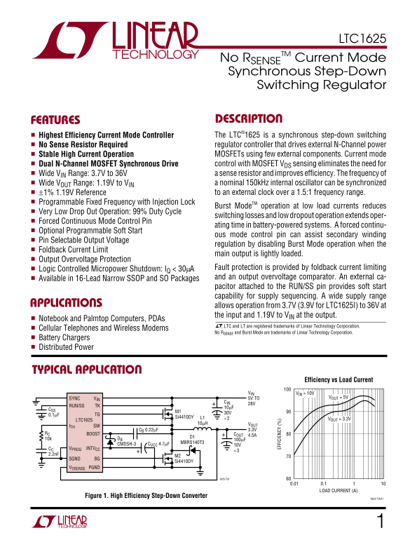
FEATURES DESCRIPTION Highest Efficiency Current Mode Controller The LTC®1625 is a synchronous step-down switching No Sense Resistor Required regulator controller that drives external N-Channel power Stable High Current Operation MOSFETs using few external components. Current mode Dual N-Channel MOSFET Synchronous Drive control with MOSFET VDS sensing eliminates the need for Wide VIN Range: 3.7V to 36V a sense resistor and improves efficiency. The frequency of Wide VOUT Range: 1.19V to VIN a nominal 150k Hz internal oscillator can be synchronized ±1% 1.19V Reference to an external clock over a 1.5:1 frequency range.

Programmable Fixed Frequency with Injection Lock

Burst Mode TM operation at low load currents reduces

Very Low Drop Out Operation: 99% Duty Cycle

switching losses and low dropout operation extends oper-

Forced Continuous Mode Control Pin

ating time in battery-powered systems. A forced continu-

Optional Programmable Soft Start

ous mode control pin can assist secondary winding

Pin Selectable Output Voltage

regulation by disabling Burst Mode operation when the

Foldback Current Limit

main output is lightly loaded.

Output Overvoltage Protection

Logic Controlled Micropower Shutdown: IQ < 30µA Fault protection is provided by foldback current limiting Available in 16-Lead Narrow SSOP and SO Packages and an output overvoltage comparator. An external ca-

EF FI CI EN CY

pacitor attached to the RUN/SS pin provides soft start capability for supply sequencing. A wide supply range

APPLICATIONS allows operation from 3.7V (3.9V for LTC1625I) to 36V at

the input and 1.19V to VIN at the output.

Notebook and Palmtop Computers, PDAs

, LTC and LT are registered trademarks of Linear Technology Corporation.

Cellular Telephones and Wireless Modems

No RSENSE and Burst Mode are trademarks of Linear Technology Corporation.

Battery Chargers Distributed Power

TYPICAL APPLICATION

Efficiency vs Load Current

VIN VIN = 10V

SYNC VIN 5V TO VOUT = 5V

RUN/SS TK

0.1µF TG

Si4410DY L1 ×2

LTC1625 VOUT = 3.3V

10µH VOUT

ITH SW

CB 0.22µF 3.3V

RC BOOST COUT

10k DB 100µF

MBRS140T3

CMDSH-3 CVCC 4.7µF 10V

CC VPROG INTVCC

SGND BG

Si4410DY

VOSENSE PGND

0.01 0.1 LOAD CURRENT (A)

Figure 1. High Efficiency Step-Down Converter

1625 TA01

Page Summary Contents For LINEAR TECHNOLOGY LTC1625 No RSENSE TM Current Mode Synchronous Step-Down Switching Regulator

Page 1 LTC1625 TM Current Mode No RSENSE Synchronous Step-Down Switching Regulator FEATURES DESCRIPTION Highest Efficiency Current Mode Controller The LTC®1625 is a synchronous step-down switching No Sense R...
Page 2 LTC1625 ABSOLUTE MAXIMUM RATINGS PACKAGE/ORDER FOR ATIO (Note 1) ORDER PART Input Supply Voltage (VIN, TK) 36V to –0.3V TOP VIEW NUMBER Boosted Supply Voltage (BOOST) 42V to –0.3V EXTVCC VIN Boosted D...
Page 3 LTC1625 TA = 25°C, VIN = 15V unless otherwise noted.ELECTRICAL CHARACTERISTICS SYMBOL PARAMETER CONDITIONS MIN TYP MAX UNITS BG Transition Time BG t R Rise Time CLOAD = 3300p F ns BG t F Fall Time CLO...
Page 4 ∆V OU IN PU CU RR EN (µ A) EF FI CI EN CY LTC1625 TYPICAL PERFOR A CE CHARACTERISTICS Efficiency vs Input Voltage, Efficiency vs Input Voltage, Efficiency vs Load Current VOUT = 5V VOUT = 3.3V FIGURE ...
Page 5 FC CU RR EN (µ A) AX IM UM UR RE NT EN SE OL TA GE (m V) LTC1625 TYPICAL PERFOR A CE CHARACTERISTICS Maximum Current Sense Voltage Maximum Current Sense Voltage Oscillator Frequency vs Duty Cycle vs T...
Page 6 LTC1625 PIN FUNCTIONS EXTVCC (Pin 1): INTVCC Switch Input. When the EXTVCC Leaving VPROG open allows the output voltage to be set by voltage is above 4.7V, the switch closes and supplies an external r...
Page 7 LTC1625 FUNCTIONAL DIAGRA 15SYNC2 TA ×11 0.6V REV BOOST 0.6V SLEEP SWITCH LOGIC/ DROPOUT SW VFB gm = 1m COUNTER SHUTDOWN INTVCC DB OVERVOLTAGE +– CVCC 0.6V BG RUN/SS 1.19V REF 1.28V VIN 5.2V LDO REG V...
Page 8 LTC1625 OPERATIO Main Control Loop will attempt to turn on the top MOSFET continuously (‘’dropout’’). A dropout counter detects this condition and The LTC1625 is a constant frequency, current mode for...
Page 9 LTC1625 APPLICATIONS INFORMATION The basic LTC1625 application circuit is shown in Figure 1. The ρT is a normalized term accounting for the significant External component selection is primarily determ...
Page 10 LTC1625 APPLICATIONS INFORMATION Top Duty Cycle IN IN OUT Bottom Duty Cycle The MOSFET power dissipations at maximum output current are: Figure 4. SYNC Clock Waveform OUT MAX DS ON  IN  Inductor V...
Page 11 LTC1625 APPLICATIONS INFORMATION The corresponding average current depends on the amount maximum values for RDS(ON), but not a minimum. A of ripple current. Lower inductor values (higher ∆IL) will rea...
Page 12 LTC1625 APPLICATIONS INFORMATION Ferrite designs have very low core loss and are preferred 2000 hours of life. This makes it advisable to further derate at high switching frequencies, so design goals ...
Page 13 LTC1625 APPLICATIONS INFORMATION High input voltage applications in which large MOSFETs 3. EXTVCC connected to an output-derived boost network. are being driven at high frequencies may cause the LTC16...
Page 14 LTC1625 APPLICATIONS INFORMATION Note that RDS(ON) also varies with the gate drive level. If VPROG pin is left open and the VOSENSE pin is connected to gate drives other than the 5.2V INTVCC are used,...
Page 15 LTC1625 APPLICATIONS INFORMATION then VSEC will droop. An external resistor divider from µ( CDELAY VSEC to the FCB pin sets a minimum voltage VSEC(MIN): SS )1 SS= When the voltage on RUN/SS reaches 1....
Page 16 LTC1625 APPLICATIONS INFORMATION where L1, L2, etc. are the individual losses as a percentage 4. LTC1625 VIN supply current. The VIN current is the DC of input power. It is often useful to analyze ind...
Page 17 LTC1625 APPLICATIONS INFORMATION automobile is the source of a number of nasty potential For 40% ripple current at maximum VIN the inductor transients, including load dump, reverse and double should b...
Page 18 LTC1625 APPLICATIONS INFORMATION VIN 12V TO 22V CIN EXTVCC VIN 22µF CSS 35V 0.1µF INTVCC SYNC TK ×2 Si4412DY RUN/SS SW L1 CC1 15µH LTC1625 VOUT 470p F RC OPEN FCB TG 3.3V 10k ITH BOOST CC2 DB CB 4.7µF...
Page 19 LTC1625 APPLICATIONS INFORMATION OPTIONAL 5V EXTVCC CONNECTION EXTVCC VIN CSS EXT SYNC TK M1 RUN/SS SW LTC1625 L1 OPEN FCB TG CC1 CB VIN RC ITH BOOST DB CVCC SGND INTVCC VOSENSE BG M2 D1 CIN OPEN VPRO...
Page 20 LTC1625 TYPICAL APPLICATIONS 2.5V/2.8A Adjustable Output RF 4.7Ω VIN CIN 5V TO 28V +CF EXTVCC VIN 0.1µF 22µF CSS 35V 0.1µF SYNC TK ×2 1/2 Si4920DY RUN/SS SW L1 CC1 15µH VOUT LTC1625 1n F RC OPEN FCB T...
Page 21 LTC1625 TYPICAL APPLICATIONS 3.3V/4A Fixed Output with 12V/120m A Auxiliary Output RF 4.7Ω VIN 6V TO 20V CF CIN 0.1µF 10µF 30V ×2 M1 IRLR3103 VSEC 12V T1 120m A 0.1µFVIN EXTVCC CSS RS DS R4 0.1µF EXT ...
Page 22 LTC1625 TYPICAL APPLICATIONS –5V/4.5A Positive to Negative Converter RF 4.7Ω VIN 5V TO 10V CF 0.1µF EXTVCC VIN SYNC TK 220µF FDS6670A RUN/SS SW CC1 CB LTC1625 2.2n F RC CSS FCB TG ITH BOOST CC2 DB D1 ...
Page 23 LTC1625 PACKAGE DESCRIPTION Dimensions in inches (millimeters) unless otherwise noted. GN Package 16-Lead Plastic SSOP (Narrow 0.150) (LTC DWG # 05-08-1641) 0.009 (0.229) REF 0° – 8° TYP0.007 – 0.0098...
Page 24 LTC1625 TYPICAL APPLICATION 3.3V/1.8A Fixed Output VIN CIN 5V TO 28V EXTVCC VIN 15µF 0.1µF SYNC TK 1/2 Si4936DY RUN/SS SW L1 CC1 27µH VOUT LTC1625 1n F RC OPEN FCB TG 3.3V 10k ITH BOOST CC2 DB CB 4.7µ...

Manual Details

Brand Current
Pages 24
File Size 378.39 KB
Published May 31, 2026
81 views

Enter the captcha to get the download link:

captcha

Frequently Asked Questions

What is the input voltage range for this regulator?

It supports operation from 3.7V up to 36V at the input.

Is an external current sense resistor needed?

No, it does not require a sense resistor because the control uses MOSFET V sensing.

Which operational mode is best for low load currents?

Burst Mode operation helps reduce power consumption when the circuit is lightly loaded.

What protection features are included to prevent failure?

It includes output overvoltage protection and foldback current limiting.

Can I synchronize the internal oscillator with an external clock?

Yes, the 150kHz internal oscillator can be synchronized to an external clock over a 1.5:1 frequency range.