# A B C D E F G H I J K L M N O P Q R S T U V W X Y Z

LINEAR TECHNOLOGY LTC1142 LTC1142L LTC1142HV Dual High Efficiency Synchronous Step-Down Switching Regulators Data Manual User Guide

Summary

These high-efficiency dual step-down switching regulators are engineered for demanding power delivery in space-constrained, battery-powered systems. Offering exceptional efficiency (over 95%) and constant off-time regulation, the LTC1142 series provides extremely stable 3.3V/5V outputs across a wide input voltage range (as low as 3.5V). This manual details critical parameters, operating modes, and performance characteristics, making it essential for designing portable instruments, notebook computers, and robust DC power distribution systems that require reliable, long-lasting operation.
📄 Preview PAGE OF 20

Page 1 Text Content

LTC1142/LTC1142L/LTC1142HV Dual High Efficiency Synchronous Step-Down Switching Regulators FEATURES DESCRIPTIO Dual Outputs: 3.3V and 5V or User Programmable The LTC®1142/LTC1142L/LTC1142HV are dual synchro- Ultrahigh Efficiency: Over 95% Possible nous step-down switching regulator controllers featuring Current Mode Operation for Excellent Line and Load automatic Burst Mode TM operation to maintain high efficien- Transient Response cies at low output currents. The devices are composed of two High Efficiency Maintained over 3 Decades of separate regulator blocks, each driving a pair of external Output Current complementary power MOSFETs, at switching frequencies Low Standby Current at Light Loads: 160µA/Output up to 250k Hz, using a constant off-time current mode archi- Independent Micropower Shutdown: IQ < 40µA tecture providing constant ripple current in the inductor.

Wide VIN Range: 3.5V to 20V

The operating current level for both regulators is user pro-

Very Low Dropout Operation: 100% Duty Cycle

grammable via an external current sense resistor. Wide input

Synchronous FET Switching for High Efficiency

supply range allows operation from 3.5V* to 18V (20V

Available in Standard 28-Pin SSOP

maximum). Constant off-time architecture provides low drop- out regulation limited only by the RDS(ON) of the external APPLICATIO MOSFET and resistance of the inductor and current sense resistor.

Notebook and Palmtop Computers

The LTC1142 series is ideal for applications requiring dual

Battery-Operated Digital Devices

output voltages with high conversion efficiencies over a wide

Portable Instruments

load current range in a small amount of board space.

DC Power Distribution Systems

, LTC and LT are registered trademarks of Linear Technology Corporation. Burst Mode is a trademark of Linear Technology Corporation.

TYPICAL APPLICATIO

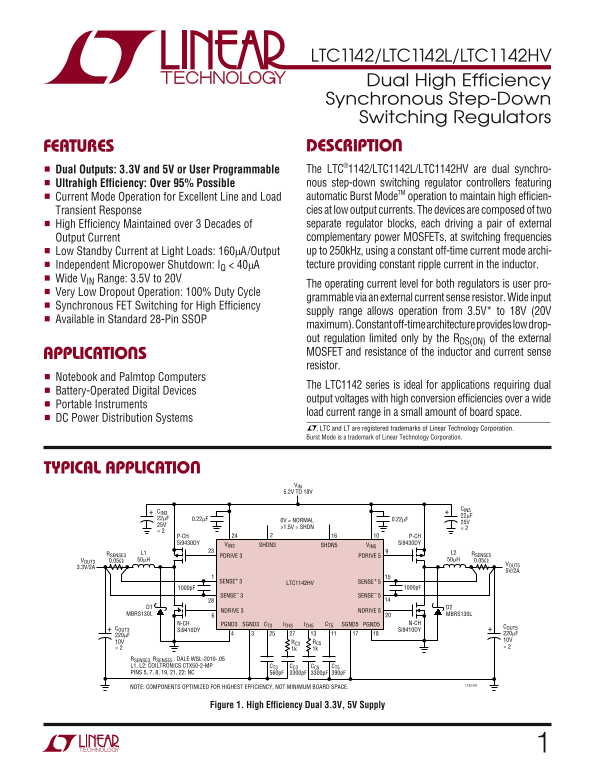
VIN 5.2V TO 18V

0V = NORMAL 25V

>1.5V = SHDN × 2

P-CH P-CH Si9430DY VIN3 Si9430DY

SHDN3 SHDN5 VIN5

RSENSE3 L1 L2 RSENSE5

PDRIVE 3 PDRIVE 5

0.05ΩVOUT3 50µH 50µH 0.05Ω

VOUT5

SENSE+ 3 LTC1142HV SENSE+ 5

SENSE– 3 SENSE– 5

NDRIVE 3 NDRIVE 5

MBRS130L MBRS130L

N-CH PGND3 SGND3 CT3 ITH3 ITH5 CT5 SGND5 PGND5 N-CH

COUT3 COUT5

Si9410DY Si9410DY

RC3 RC5

RSENSE3, RSENSE5 : DALE WSL-2010-.05 L1, L2: COILTRONICS CTX50-2-MP CT3 CC3 CC5 CT5 PINS 5, 7, 8, 19, 21, 22: NC 560p F 3300p F 3300p F 390p F

1142 F01NOTE: COMPONENTS OPTIMIZED FOR HIGHEST EFFICIENCY, NOT MINIMUM BOARD SPACE.

Figure 1. High Efficiency Dual 3.3V, 5V Supply

Page Summary Contents For LINEAR TECHNOLOGY LTC1142 LTC1142L LTC1142HV Dual High Efficiency Synchronous Step-Down Switching Regulators Data Manual User Guide

Page 1 LTC1142/LTC1142L/LTC1142HV Dual High Efficiency Synchronous Step-Down Switching Regulators FEATURES DESCRIPTIO Dual Outputs: 3.3V and 5V or User Programmable The LTC®1142/LTC1142L/LTC1142HV are dual s...
Page 2 LTC1142/LTC1142L/LTC1142HV ABSOLUTE AXI RATI GS (Note 1) Input Supply Voltage (Pins 10, 24) Operating Ambient Temperature Range 0°C to 70°C LTC1142, LTC1142L-ADJ 16V to –0.3V Extended Commercial LTC11...
Page 3 LTC1142/LTC1142L/LTC1142HV ELECTRICAL CHARACTERISTICS The ● denotes the specifications which apply over the full operating temperature range, otherwise specifications are at TA = 25°C. V10 = V24 = 10V...
Page 4 EF FI CI EN CY EF FI CI EN CY LTC1142/LTC1142L/LTC1142HV ELECTRICAL CHARACTERISTICS –40°C ≤ TA ≤ 85°C (Note 5), V10 = V24 = 10V, unless otherwise noted. SYMBOL PARAMETER CONDITIONS MIN TYP MAX UNITS L...
Page 5 GA TE HA RG CU RR EN (m A) SU PP LY UR RE NT (m A) LTC1142/LTC1142L/LTC1142HV TYPICAL PERFOR A CE CHARACTERISTICS Operating Frequency vs DC Supply Current Supply Current in Shutdown VIN – VOUT 2.1 1.6...
Page 6 LTC1142/LTC1142L/LTC1142HV PI FU CTIO NC (Pins 7, 8): No Connection. NC (Pins 21, 22): No Connection. PDRIVE 5 (Pin 9): High Current Drive for Top P-Channel PDRIVE 3 (Pin 23): High Current Drive for T...
Page 7 LTC1142/LTC1142L/LTC1142HV PI FU CTIO NDRIVE 1 (Pin 6): High Current Drive for Bottom N-Channel SGND2 (Pin 18): The section 2 small-signal ground must MOSFET, Section 1. Voltage swing at Pin 6 is from...
Page 8 LTC1142/LTC1142L/LTC1142HV FU CTIO AL DIAGRA Only one regulator block shown. Pin numbers are for 3.3V (5V) sections for LTC1142/LTC1142HV, and VOUT1 (VOUT2) for LTC1142L-ADJ/LTC1142HV-ADJ. PIN NUMBERS...
Page 9 LTC1142/LTC1142L/LTC1142HV OPERATIO Refer to Functional Diagram As the load current increases, the output voltage de- hysteresis in comparator V, the P-channel MOSFET is creases slightly. This causes ...
Page 10 LTC1142/LTC1142L/LTC1142HV APPLICATIO S I FOR ATIO EN SE (Ω both track IMAX. Once RSENSE has been chosen, IBURST and A graph for selecting CT versus frequency including the ISC(PK) can be predicted fr...
Page 11 LTC1142/LTC1142L/LTC1142HV APPLICATIO S I FOR ATIO eased at the expense of efficiency. If too small an inductor The minimum input voltage determines whether standard is used, the inductor current will...
Page 12 LTC1142/LTC1142L/LTC1142HV APPLICATIO S I FOR ATIO dead-time, which could cost as much as 1% in efficiency from Sanyo has the lowest ESR/size ratio of any aluminum (although there are no other harmful...
Page 13 LTC1142/LTC1142L/LTC1142HV APPLICATIO S I FOR ATIO current. When a load step occurs, VOUT shifts by an section) less the gate charge current. For VIN = 10V the amount equal to ∆ILOAD • ESR, where ESR ...
Page 14 LTC1142/LTC1142L/LTC1142HV EF FI CI EN CY /L OS APPLICATIO S I FOR ATIO Figure 5 shows how the efficiency losses in one section of and δP = δN = 0.007(63 – 25) = 0.27. The required RDS(ON) a typical L...
Page 15 LTC1142/LTC1142L/LTC1142HV APPLICATIO S I FOR ATIO To prevent stray pickup a 100p F capacitor is suggested the layout diagram of Figure 7. In general each block across R1 located close to the LTC1142H...
Page 16 LTC1142/LTC1142L/LTC1142HV APPLICATIO S I FOR ATIO ing with Kelvin connections. Be sure to use a PCB PIN 26(12) INT VCC FROM CROWBAR pattern similar to that shown in Figure 7 for the current DETECT CI...
Page 17 LTC1142/LTC1142L/LTC1142HV APPLICATIO S I FOR ATIO may be loaded without regard to the primary output load, With the addition of R3 a current is generated through R1 providing that the loop remains in...
Page 18 LTC1142/LTC1142L/LTC1142HV TYPICAL APPLICATIO VIN 4.5V TO 18V 0V = NORMAL &gt;1.5V = SHDN × 2 P-CH P-CH Si9430DY Si9430DY VIN1 SHDN1 SHDN2 VIN2 RSENSE1 L1 L2 RSENSE2 33µH PDRIVE 1 PDRIVE 2 VOUT1 VOUT2...
Page 19 LTC1142/LTC1142L/LTC1142HV TYPICAL APPLICATIO VIN 6.5V TO 0V = NORMAL 14V 1µF &gt;1.5V = SHDN P-CH P-CH Si9430DY VIN3 Si9430DY T1 SHDN3 SHDN5 VIN5 RSENSE3 L1 RSENSE5 PDRIVE 3 PDRIVE 5 0.05ΩVOUT3 33µH ...
Page 20 LTC1142/LTC1142L/LTC1142HV TYPICAL APPLICATIO OU TP UT UR RE NT (m A) SET RESISTANCE (kΩ) Figure 16. LTC1142HV-ADJ Output Current vs Trickle Charge Set Resistance (RX) for the Circuit in Figure 15 Usi...

Manual Details

Brand Linear
Pages 20
File Size 248.17 KB
Published June 17, 2026
7 views

Enter the captcha to get the download link:

captcha

Frequently Asked Questions

What is the maximum efficiency of this step-down regulator?

It offers Ultrahigh Efficiency, exceeding 95%.

Does it function correctly at low loads or during standby?

Yes, it features a constant off-time architecture with a low standby current below 40mA.

What is the supported input voltage range for this device?

The operating range allows operation from 3.5V up to 20V (LTC1142HV).

What types of applications are ideal for the LTC1142 series?

It is ideal for notebooks, portable instruments, and DC power distribution needing dual voltage outputs.