# A B C D E F G H I J K L M N O P Q R S T U V W X Y Z

LINEAR TECHNOLOGY - LTC3555 High Efficiency USB Power Manager + Triple Step-Down DC-DC Manual

Summary

Linear Technology LTC3555 USB power manager with triple DC/DC converter. Integrates PowerPath controller, 1.5A Li-Ion charger, ideal diode, and three step-down regulators (1A/400mA/400mA). Supports USB current limits, I2C control, and voltage scaling in 28-pin QFN. For portable device power management engineers.
📄 Preview PAGE OF 32

Page 1 Text Content

LTC3555/LTC3555-X High Effi ciency USB Power Manager + Triple Step-Down DC/DC

FEATURES DESCRIPTION Power Manager The LTC®3555 family are highly integrated USB com- n High Effi ciency Switching Power Path™ Controller

patible power management and battery charger ICs for

with Bat-Track™ Adaptive Output Control Li-Ion/Polymer battery applications. They include a high n Programmable USB or Wall Current Limit

effi ciency current limited switching Power Path manager

(100m A/500m A/1A) with automatic load prioritization, a battery charger, an ideal n Full Featured Li-Ion/Polymer Battery Charger

diode and three general purpose synchronous step-down

n 1.5A Maximum Charge Current

switching regulators.

n Internal 180mΩ Ideal Diode + External Ideal Diode

The LTC3555 family limits input current to either 100m A

Controller Powers Load in Battery Mode

or 500m A for USB applications or 1A for adapter-powered

n Low No-Load Quiescent Current when Powered from

applications. Unlike linear chargers, the LTC3555 family’s

BAT (<32μA)

switching architecture transmits nearly all of the power avail-

DC/DCs

able from the USB port to the load with minimal loss and

n Triple High Effi ciency Step-Down DC/DCs

heat which eases thermal constraints in small spaces.

(1A/400m A/400m A IOUT)

Two of the three general purpose switching regulators can

n All Regulators Operate at 2.25MHz

provide up to 400m A and the third can deliver 1A. The

n Dynamic Voltage Scaling on Two Outputs

entire product can be controlled via I2C or simple I/O. The

n I2C or Independent Enable, VOUT Controls

LTC3555-1/LTC3555-3 versions offer “instant-on” power

n Low No-Load Quiescent Current: 20μA

FF IC IE delivery to the portable product even with a very low battery

n 28-Pin (4mm × 5mm × 0.75mm) QFN Package

voltage. The LTC3555-3 version also has a reduced charger fl oat voltage of 4.100V for battery safety and longevity.

APPLICATIONS

The LTC3555 family is available in the low profi le 28-pin

n HDD-Based MP3 Players, PDAs, GPS, PMPs

(4mm × 5mm × 0.75mm) QFN surface mount package.

n Portable Medical Products

L, LT, LTC and LTM are registered trademarks of Linear Technology Corporation. Power Path n Handheld Instrumentation and Bat-Track are trademarks of Linear Technology Corporation. All other trademarks are the property of their respective owners. Protected by U.S. Patents, including 6522118 and 6404251.

n Other USB-Based Handheld Products

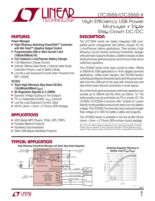
TYPICAL APPLICATION High Effi ciency Power Path Manager and Triple Step-Down Regulator

Switching Regulator Effi ciency to

USB/WALL TO OTHER

USB COMPLIANT System Load (POUT/PBUS)

4.35V TO 5.5V LOADS

STEP-DOWN REGULATOR

CC/CV

OPTIONAL0V

BATTERY

CURRENT

CHARGER

CONTROL

BAT = 4.2V

CHARGE

Li-Ion

LTC3555/LTC3555-X BAT = 3.3V

3.3V/25m A RTC/LOW

ALWAYS ON LDO

POWER LOGIC

0.8V TO 3.6V/400m A

TRIPLE MEMORY

ENABLE HIGH EFFICIENCY 0.8V TO 3.6V/400m A VBUS = 5V

STEP-DOWN I/O

CONTROLS IBAT = 0m A

SWITCHING 0.8V TO 3.6V/1A 10x MODE

REGULATORS

μPROCESSOR 0.01 0.1 IOUT (A)

I2C PORT I2C

3555 TA01b

3555 TA01

3555fd

Page Summary Contents For LINEAR TECHNOLOGY - LTC3555 High Efficiency USB Power Manager + Triple Step-Down DC-DC Manual

Page 1 LTC3555/LTC3555-X High Effi ciency USB Power Manager + Triple Step-Down DC/DC FEATURES DESCRIPTION Power Manager The LTC®3555 family are highly integrated USB com- n High Effi ciency Switching Power P...
Page 2 LTC3555/LTC3555-X ABSOLUTE MAXIMUM RATINGS PIN CONFIGURATION (Notes 1, 2, 3) VBUS (Transient) t &lt; 1ms, TOP VIEW Duty Cycle &lt; 1% .......................................... –0.3V to 7V VIN1, VIN2,...
Page 3 LTC3555/LTC3555-X ELECTRICAL CHARACTERISTICS The l denotes the specifi cations which apply over the full operating temperature range, otherwise specifi cations are at TA = 25°C. VBUS = 5V, BAT = 3.8V,...
Page 4 LTC3555/LTC3555-X ELECTRICAL CHARACTERISTICS The l denotes the specifi cations which apply over the full operating temperature range, otherwise specifi cations are at TA = 25°C. VBUS = 5V, BAT = 3.8V,...
Page 5 LTC3555/LTC3555-X ELECTRICAL CHARACTERISTICS The l denotes the specifi cations which apply over the full operating temperature range, otherwise specifi cations are at TA = 25°C. VBUS = 5V, BAT = 3.8V,...
Page 6 LTC3555/LTC3555-X ELECTRICAL CHARACTERISTICS The l denotes the specifi cations which apply over the full operating temperature range, otherwise specifi cations are at TA = 25°C. VBUS = 5V, BAT = 3.8V,...
Page 7 FF IC IE LTC3555/LTC3555-X TYPICAL PERFORMANCE CHARACTERISTICS Ideal Diode Resistance Output Voltage vs Output Current Ideal Diode V-I Characteristics vs Battery Voltage (Battery Charger Disabled) INT...
Page 8 FR z) LT LTC3555/LTC3555-X TYPICAL PERFORMANCE CHARACTERISTICS Output Voltage vs Load Current in VBUS Current vs Load Current in 3.3V LDO Output Voltage vs Load Suspend Suspend Current, VBUS = 0V VBUS...
Page 9 IN -R IS TA T3 IN LTC3555/LTC3555-X TYPICAL PERFORMANCE CHARACTERISTICS RST3, CHRG Pin Current vs 3.3V LDO Step Response Battery Drain Current vs Voltage (Pull-Down State) (5m A to 15m A) Temperature ...
Page 10 LT FF IC IE FF IC IE LTC3555/LTC3555-X TYPICAL PERFORMANCE CHARACTERISTICS Switching Regulators 1, 2 Switching Regulators 1, 2 Switching Regulators 1, 2 Pulse Skip Mode Effi ciency Burst Mode Effi cie...
Page 11 LTC3555/LTC3555-X PIN FUNCTIONS LDO3V3 (Pin 1): 3.3V LDO Output Pin. This pin provides DVCC (Pin 8): Logic Supply for the I2C Serial Port. If the a regulated always-on 3.3V supply voltage. LDO3V3 seri...
Page 12 LTC3555/LTC3555-X PIN FUNCTIONS SW1 (Pin 17): Power Transmission Pin for Switching BAT (Pin 23): Single Cell Li-Ion Battery Pin. Depending on Regulator 1. available VBUS power, a Li-Ion battery on BAT...
Page 13 LTC3555/LTC3555-X BLOCK DIAGRAM 25VBUS 2.25MHz Power Path SWITCHING REGULATOR LDO3V31 3.3V LDO SUSPEND LDO VOUT CC/CV IDEAL GATE 2CLPROG CHARGER BATTERY BAT 3NTC TEMPERATURE MONITOR PROG 21CHRG ENABLE...
Page 14 LTC3555/LTC3555-X TIMING DIAGRAM DATA BYTE A DATA BYTE B ADDRESS WR STOPSTART SDA ACK ACK ACK t SU, DAT t SU, STA t BUF t LOW t HD, DAT t HD, STA t SU, STO 3555 TD t HD, STA t HIGH t SP START REPEATED...
Page 15 LTC3555/LTC3555-X OPERATION If the combined load at VOUT is large enough to cause the switching power supply to reach the programmed input 4.2 current limit, the battery charger will reduce its charge...
Page 16 LTC3555/LTC3555-X OPERATION If the load current increases beyond the power allowed at BAT. The resistance of the internal ideal diode is approxi- from the switching regulator, additional power will be...
Page 17 LTC3555/LTC3555-X OPERATION specifi cation. If the load on VOUT exceeds the suspend current delivered to the battery will try to reach 1022V/ current limit, the additional current will come from the R...
Page 18 LTC3555/LTC3555-X OPERATION 1022 times the current in the PROG pin. The program duty cycles are disparate enough to make an LED appear resistor and the charge current are calculated using the to be on...
Page 19 LTC3555/LTC3555-X OPERATION duty cycle reading will be precisely 50%. If the duty cycle than worst-case conditions with the assurance that the reading is 50%, system software should disqualify it and ...
Page 20 LTC3555/LTC3555-X OPERATION Table 2. I2C Serial Port Mapping A7 A6 A5 A4 A3 A2 A1 A0 B7 B6 B5 B4 B3 B2 B1 B0 Switching Regulator 2 Switching Regulator 3 Disable Switching Enable Enable Enable Input Cu...
Page 21 LTC3555/LTC3555-X OPERATION the LTC3555 family will remember the last input of valid remains low impedance until regulator 3 reaches 92% of data that it received. Once all chips on the bus have been i...
Page 22 LTC3555/LTC3555-X OPERATION Step-Down Switching Regulator Output Voltage turn off and the N-channel MOSFET synchronous rectifi er Programming to turn on. The N-channel MOSFET synchronous rectifi er tu...
Page 23 LTC3555/LTC3555-X OPERATION operation provides a signifi cant improvement in effi ciency nanoamperes of leakage current. The step-down switch- at light loads at the expense of higher output ripple whe...
Page 24 LTC3555/LTC3555-X APPLICATIONS INFORMATION CLPROG Resistor and Capacitor The LTC3555 family includes a current-reversal comparator which monitors inductor current and disables the synchro- As describe...
Page 25 LTC3555/LTC3555-X APPLICATIONS INFORMATION by application. Some inductors that may be suitable for over their rated voltage and temperature ranges. Y5V this application are listed in Table 6. ceramic ...
Page 26 LTC3555/LTC3555-X APPLICATIONS INFORMATION small and don’t radiate much energy, but generally cost General Purpose Switching Regulator Input/Output more than powdered iron core inductors with similar ...
Page 27 LTC3555/LTC3555-X APPLICATIONS INFORMATION Alternate NTC Thermistors and Biasing VBUSVBUS LTC3555/LTC3555-X NTC BLOCK The LTC3555 family provides temperature qualifi ed charg- 0.765 • VBUS RNOM ing if...
Page 28 LTC3555/LTC3555-X APPLICATIONS INFORMATION RNTC|COLD = 3.25 • RNOM the nearest 1% value is 10.5k: By setting RNOM equal to R25, the above equations result R1 = 0.536 • 10.5k – 0.4368 • 10k = 1.26k in ...
Page 29 LTC3555/LTC3555-X APPLICATIONS INFORMATION MP1 Si2333 C1 5V USB 100n F LTC3555/ INPUT C2 USB CABLE LTC3555-X Figure 6. USB Soft Connect Circuit the IC and all of its external high frequency components...
Page 30 LTC3555/LTC3555-X TYPICAL APPLICATION Watchdog Microcontroller Operation USB/WALL TO OTHER SWVBUS 4.5V TO 5.5V LOADS 10k VOUT NTC GATE MP1 PROG BAT 2k CLPROG Li-Ion 8.2Ω GND 3k 0.1μF SW1 MEMORY FB1LDO...
Page 31 LTC3555/LTC3555-X PACKAGE DESCRIPTION UFD Package 28-Lead Plastic QFN (4mm × 5mm) (Reference LTC DWG # 05-08-1712 Rev B) 2.50 REF PACKAGE OUTLINE 0.25 ±0.05 0.50 BSC 3.50 REF 4.10 ± 0.05 5.50 ± 0.05 R...
Page 32 LTC3555/LTC3555-X TYPICAL APPLICATION Push Button Start with Automatic Sequencing, Reverse Input Voltage Protection and 10 Second Push and Hold Hard Shutdown MP1USB VBUS SW1 MEMORY CONNECTOR DVCC 0.1μ...

Manual Details

Brand Linear
Pages 32
File Size 309.51 KB
Published June 15, 2026
6 views

Enter the captcha to get the download link:

captcha

Frequently Asked Questions

What are the output currents of the three step-down DC/DCs?

Two can deliver 400mA, and the third can deliver 1A.

What is the operating temperature range of the LTC3555?

The operating temperature range is -40°C to 85°C.

What USB input current limits does the LTC3555 support?

It supports 100mA and 500mA for USB, and 1A for adapter-powered applications.

What package does the LTC3555 family use?

It uses a 28-pin 4mm × 5mm × 0.75mm QFN surface mount package.