# A B C D E F G H I J K L M N O P Q R S T U V W X Y Z

LINEAR Low Input Voltage, High Power Synchronous Buck DC-DC Controller User's Manual

Summary

The LTC3713 is a high-efficiency synchronous buck DC/DC controller engineered for advanced power management in space-constrained applications, such as telecom or portable devices. This versatile regulator excels at high current efficiency while supporting extremely low input voltages as little as 1.5V, eliminating the need for a sense resistor. The associated manual provides comprehensive technical documentation, covering detailed electrical characteristics, operational parameters, and application guidelines required for reliable integration into demanding point-of-load power circuits.
📄 Preview PAGE OF 24

Page 1 Text Content

查询LTC3711EGN供应商

LTC3713

Low Input Voltage,

High Power, No RSENSE

Synchronous Buck DC/DC Controller

FEATURES DESCRIPTIO

Very Low VIN(MIN): 1.5V The LTC®3713 is a high current, high efficiency synchro- True Current Mode Control nous buck switching regulator controller optimized for 5V Drive for N-Channel MOSFETs Eliminates use with very low input supply voltages. It operates from Auxillary 5V Supply inputs as low as 1.5V and provides a regulated output No Sense Resistor Required voltage from 0.8V up to (0.9)VIN. The controller uses Uses Standard 5V Logic-Level N-Channel MOSFETs a valley current control architecture to enable high operat- Adjustable Current Limit ing frequencies without requiring a sense resistor. Adjustable Frequency Operating frequency is selected by an external resistor and Switch t ON(MIN) < 100ns is compensated for variations in VIN and VOUT. The LTC3713 2% to 90% Duty Cycle at 200k Hz uses a pair of standard 5V logic-level N-channel external 0.8V ±1% Reference MOSFETs, eliminating the need for expensive P-channel Power Good Output Voltage Monitor or low threshold devices.

Programmable Soft-Start

Discontinuous mode operation provides high efficiency

Output Overvoltage Protection

operation at light loads. A forced continuous control

Optional Short-Circuit Shutdown Timer

pin reduces noise and RF interference, and can assist

Small 24-Lead SSOP Package

secondary winding regulation by disabling discontinuous

EF FI CI EN CY operation when the main output is lightly loaded. Fault

APPLICATIO S

protection is provided by internal foldback current limit- Telecom Card 3.3V, 2.5V, 1.8V Step-Down ing, an output overvoltage comparator and an optional Bus Termination (DDR memory, SSTL) short-circuit shutdown timer.

Synchronous Buck with General Purpose Boost

, LTC and LT are registered trademarks of Linear Technology Corporation. Low VIN Synchronous Boost No RSENSE is a trademark of Linear Technology Corporation.

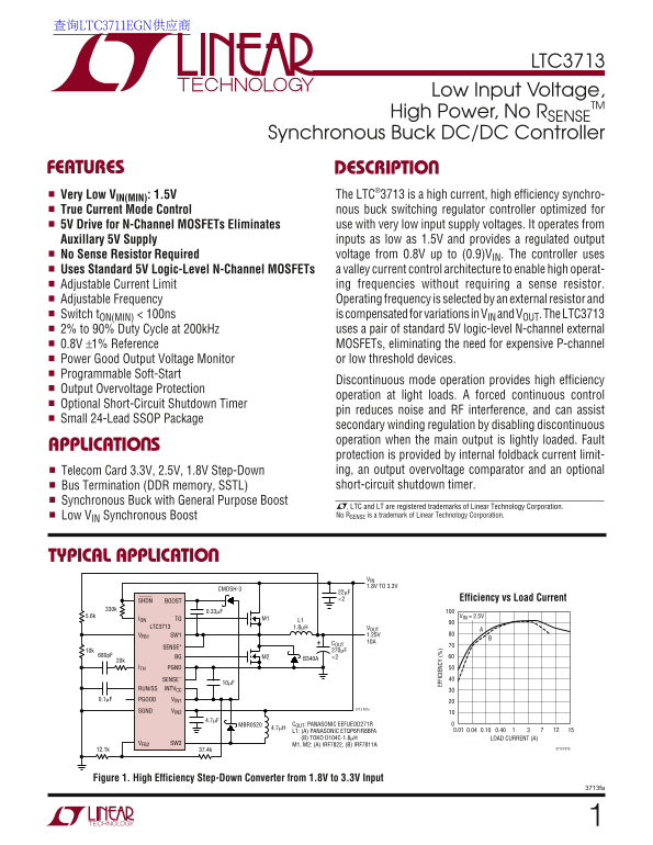
TYPICAL APPLICATIO

VIN 1.8V TO 3.3V

CMDSH-3

22µF SHDN BOOST ×2 Efficiency vs Load Current

5.6k VIN = 2.5V

ION TG M1 L1

LTC3713 1.8µH VOUT

VFB1 SW1 1.25V COUT 10A

SENSE+

680p F BG M2 ×2

ITH PGND

SENSE–

RUN/SS INTVCC

0.1µF PGOOD VIN1

SGND VIN2

COUT: PANASONIC EEFUEOD271R 4.7µHMBR0520 0.01

L1: (A) PANASONIC ETQP6FIR8BFA 0.04 0.10 0.40

(B) TOKO D104C-1.8µH LOAD CURRENT (A)

VFB2 SW2 M1, M2: (A) IRF7822, (B) IRF7811A

Figure 1. High Efficiency Step-Down Converter from 1.8V to 3.3V Input

3713fa

Page Summary Contents For LINEAR Low Input Voltage, High Power Synchronous Buck DC-DC Controller User's Manual

Page 1 查询LTC3711EGN供应商 LTC3713 Low Input Voltage, High Power, No RSENSE Synchronous Buck DC/DC Controller FEATURES DESCRIPTIO Very Low VIN(MIN): 1.5V The LTC®3713 is a high current, high efficiency synchro- ...
Page 2 LTC3713 ABSOLUTE AXI U RATI GS PACKAGE/ORDER I FOR ATIO (Note 1) Input Supply Voltage (VIN2) .......................10V to –0.3V TOP VIEW ORDER PART Boosted Topside Driver Supply Voltage NUMBER RUN/SS...
Page 3 LTC3713 ELECTRICAL CHARACTERISTICS The ● denotes specifications which apply over the full operating temperature range, otherwise specifications are TA = 25°C. VIN1 = 15V, VIN2 = 1.5V unless otherwise ...
Page 4 SW IT CH IN FR EQ UE NC (M Hz FE ED BA CK IN OL TA GE (V LTC3713 TYPICAL PERFOR A CE CHARACTERISTICS Transient Response (Discontinuous Mode)Transient Response Start-Up from Shutdown VOUT VOUT 100m V/D...
Page 5 AX IM UM UR RE NT EN SE HR ES HO LD (m V) ON -T IM (n s) ∆V OU LTC3713 TYPICAL PERFOR A CE CHARACTERISTICS Frequency vs Input Voltage Load Regulation On-Time vs ION Current 10k VVON = 0V LOAD = 6A LOA...
Page 6 CU RR EN SE NS TH RE SH OL (m V) FE ED BA CK EF ER EN CE OL TA GE (V LTC3713 TYPICAL PERFOR A CE CHARACTERISTICS RU N/ SS HR ES HO LD (V Feedback Reference Voltage vs Error Amplifier gm vs INTVCC Load...
Page 7 LTC3713 PI FU CTIO S RUN/SS (Pin 1): Run Control and Soft-Start Input. A VFB2 (Pin 12): Boost Converter Feedback. The VFB2 pin is capacitor to ground at this pin sets the ramp time to full connected t...
Page 8 LTC3713 FU CTIO AL DIAGRA S VON VIN ION FCB VIN1 0.8V REF 5V REG BOOST VVON t ON = (10p F) CB IION TG FCNT M1 SENSE+ L1 SWITCH ICMP IREV DB VOUT LOGIC INTVCC 1.4V CVCC COUT PGND1 SENSE– PGOOD Q2 Q4 UV...
Page 9 LTC3713 OPERATIO Main Control Loop and M2 is turned on and held on until the overvoltage condition clears. The LTC3713 is a current mode controller for DC/DC step-down converters designed to operate f...
Page 10 LTC3713 OPERATIO switch cycle, turning on the switch. When the summation response can be optimized by the addition of a phase lead of a signal representing switch current and a ramp gen- capacitor CPL...
Page 11 LTC3713 APPLICATIO S I FOR ATIO SENSE+ The gate drive voltage is set by the 5V INTVCC supply. WITHOUT RSENSE Consequently, logic-level threshold MOSFETs must be used in LTC3713 applications. SENSE+ Wh...
Page 12 LTC3713 APPLICATIO S I FOR ATIO The resulting power dissipation in the MOSFETs at maxi- Hz OUT mum output current are: VON ON 2 ρT(TOP) RDS(ON)(MAX) PTOP = DTOP IOUT(MAX) To hold frequency constant du...
Page 13 LTC3713 APPLICATIO S I FOR ATIO specific application. A good starting point is to feed about of the bottom MOSFET from turning on and storing charge 25% of the voltage change at the ITH pin to the VON...
Page 14 LTC3713 APPLICATIO S I FOR ATIO Tantalum capacitors have the highest capacitance density Fault Conditions: Current Limit and Foldback but it is important to only use types that have been surge The max...
Page 15 LTC3713 APPLICATIO S I FOR ATIO due to a dropping input voltage for example, then the SS µ( )1 CDELAY SS= output will drop out of regulation. The minimum input voltage to avoid dropout is: When the vo...
Page 16 LTC3713 APPLICATIO S I FOR ATIO be estimated from: converter. To ensure that the ripple current doesn’t exceed a specified amount, the inductance can be chosen accord- CSS &gt; COUT • VOUT • RSENSE (1...
Page 17 LTC3713 APPLICATIO S I FOR ATIO loss. For example, if RDS(ON) = 0.01Ω and RL = 0.005Ω, the Design Example loss will range from 1% up to 10% as the output current As a design example, take a supply wit...
Page 18 LTC3713 APPLICATIO S I FOR ATIO However, a 0A to 6A load step will cause an output change of up to: ∆VOUT(STEP) = ∆ILOAD (ESR) = (6A) (0.005Ω) = 30m V p F k Hz The inductor for the boost converter is ...
Page 19 LTC3713 APPLICATIO S I FOR ATIO PC Board Layout Checklist Flood all unused areas on all layers with copper. Flooding with copper will reduce the temperature rise When laying out a PC board follow one ...
Page 20 LTC3713 TYPICAL APPLICATIO S 1.25V/±6A Bus Terminator RPG DB 100k CMDSH-3 VIN RUN/SS BOOST 2.5V CB TO 3.3V M1 B340A CIN1B VON TG IRF7811A 330µF CIN1A 22µF PGOOD PGOOD SW1 X5R 6.3V VRNG SENSE+ L1 ×2 VO...
Page 21 LTC3713 TYPICAL APPLICATIO S One-Half VIN/±6A Bus Terminator VIN CINA 1.8V TO 3.3V CINB CMDSH-3 RPG RUN/SS BOOST VON TG IRF7811A PGOOD PGOOD SW1 VRNG SENSE+ R1 R3 1µH VOUT 10k 5k 0.9V TO 1.65V D3 FCB ...
Page 22 LTC3713 TYPICAL APPLICATIO S Dual Output 1.25V/10A Buck Converter and 5V to 12V/130m A Boost Converter CSS RF DB 0.1µF 1Ω CMDSH-3 RUN/SS BOOST CB CINIA 5V TO 24V VON TG X5R IRF7811A PGOOD PGOOD SW1 VR...
Page 23 LTC3713 PACKAGE DESCRIPTIO G Package 24-Lead Plastic SSOP (5.3mm) (Reference LTC DWG # 05-08-1640) 0.42 ±0.03 0.65 BSC RECOMMENDED SOLDER PAD LAYOUT BSC 0.05 NOTE: (.002) G24 SSOP 0802 1. CONTROLLING ...
Page 24 LTC3713 TYPICAL APPLICATIO 3.3V to 5V Synchronous Boost Converter RPG DB L1 100k CMDSH-3 1.8µH RUN/SS BOOST CB 3.3V 0.33µF CINIA CINIB VON TG 22µF PGOOD PGOOD SW1 IRF7811A VOUT VRNG SENSE+ 5V 52.5k D1...

Manual Details

Brand High Power
Pages 24
File Size 309.50 KB
Published May 28, 2026
73 views

Enter the captcha to get the download link:

captcha

Frequently Asked Questions

What are the minimum input voltage requirements for the LTC3713?

It operates from auxiliary supplies as low as 1.5V, and its regulated output can handle inputs from 0.8V up to 0.9V.

Does this DC/DC controller require a sense resistor?

No, the device is designed without requiring an external sense resistor (No R).

What operational protection features are built into the chip?

It includes internal foldback current limit, Output Overvoltage Protection, and optional Short-Circuit Shutdown.

How can I adjust the operating frequency of the controller?

The running operating frequency is adjusted by selecting an external resistor.