# A B C D E F G H I J K L M N O P Q R S T U V W X Y Z

LINEAR TECHNOLOGY LTC3709 Fast 2-Phase, No RSENSE Synchronous DC DC Controller with Tracking Sequencing

Summary

The LTC3709 is a high-efficiency, single output dual-phase synchronous step-down switching regulator designed for advanced power management systems. Its key features include external clock synchronization, optional sensing resistor functionality, and precise tracking/sequencing capabilities. This manual provides comprehensive details on its performance curves, robust protection schemes (OVP, short-circuit shutdown), and wide operating range. Ideal for powering components in notebook computers, DSPs, ASICs, and graphic processors requiring stable, efficient power conversion across varying loads.
📄 Preview PAGE OF 24

Page 1 Text Content

LTC3709 TM,

Fast 2-Phase, No RSENSE POW ER LOSS (W

Synchronous DC/DC Controller with Tracking/Sequencing

FEATURES DESCRIPTIO

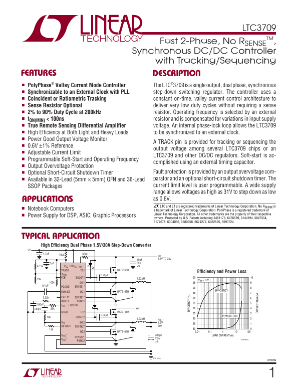
Poly Phase® Valley Current Mode Controller The LTC®3709 is a single output, dual phase, synchronous Synchronizable to an External Clock with PLL step-down switching regulator. The controller uses a Coincident or Ratiometric Tracking constant on-time, valley current control architecture to Sense Resistor Optional deliver very low duty cycles without requiring a sense 2% to 90% Duty Cycle at 200k Hz resistor. Operating frequency is selected by an external t ON(MIN) < 100ns resistor and is compensated for variations in input supply True Remote Sensing Differential Amplifier voltage. An internal phase-lock loop allows the LTC3709 High Efficiency at Both Light and Heavy Loads to be synchronized to an external clock.

Power Good Output Voltage Monitor

A TRACK pin is provided for tracking or sequencing the

0.6V ±1% Reference

output voltage among several LTC3709 chips or an

Adjustable Current Limit

LTC3709 and other DC/DC regulators. Soft-start is ac-

Programmable Soft-Start and Operating Frequency

complished using an external timing capacitor.

Output Overvoltage Protection

Optional Short-Circuit Shutdown Timer Fault protection is provided by an output overvoltage com- Available in 32-Lead (5mm × 5mm) QFN and 36-Lead parator and an optional short-circuit shutdown timer. The SSOP Packages current limit level is user programmable. A wide supply

EF FI CI EN CY

range allows voltages as high as 31V to step down as low APPLICATIO S as 0.6V. , LTC and LT are registered trademarks of Linear Technology Corporation. No RSENSE is

Notebook Computers a trademark of Linear Technology Corporation. Poly Phase is a registered trademark of

Linear Technology Corporation. All other trademarks are the property of their respective

Power Supply for DSP, ASIC, Graphic Processors

owners. Protected by U.S. Patents including 5481178, 6476589, 6144194, 5847554, 6177678, 6304066, 6580258, 6674274, 6462525, 6593724.

TYPICAL APPLICATIO High Efficiency Dual Phase 1.5V/30A Step-Down Converter 5V

VIN 4.5V TO 28V

47.5k VCC DRVCC ION ×3

TRACK TG1 HAT2168H

Efficiency and Power Loss

FCB BOOST1

VIN = 12V

100k SW1 0.1µF

PGOOD SENSE1+

EFFICIENCY

RUN/SS BG1 HAT2165H

3.32k EXTLPF SENSE1– INTLPF PGND1

100n F ITH LTC3709

20k VIN

SGND TG2 HAT2168H

POWER LOSS

10k BOOST2

1.22µH VOUT

VFB SW2 1.5V

DIFFOUT SENSE2+ 30A

BG2 HAT2165H 0.01 0.1

VOS 330µF LOAD CURRENT (A)

SENSE2–

2.5V 3709 TA01b

PGND2 ×4

3709 TA01a

3709fa

Page Summary Contents For LINEAR TECHNOLOGY LTC3709 Fast 2-Phase, No RSENSE Synchronous DC DC Controller with Tracking Sequencing

Page 1 LTC3709 TM, Fast 2-Phase, No RSENSE POW ER LOSS (W Synchronous DC/DC Controller with Tracking/Sequencing FEATURES DESCRIPTIO Poly Phase® Valley Current Mode Controller The LTC®3709 is a single output,...
Page 2 LTC3709 ABSOLUTE AXI RATI GS (Note 1) Input Supply Voltage (VCC, DRVCC) 7V to –0.3V ITH Voltage 2.7V to –0.3V Boosted Topside Driver Supply Voltage VFB Voltage 2.7V to –0.3V S+ NG (BOOST1, BOOST2) 37V...
Page 3 LTC3709 ELECTRICAL CHARACTERISTICS The ● denotes specifications which apply over the full operating temperature range, otherwise specifications are at TA = 25°C. VCC = DRVCC = 5V, unless otherwise not...
Page 4 LTC3709 ELECTRICAL CHARACTERISTICS The ● denotes specifications which apply over the full operating temperature range, otherwise specifications are at TA = 25°C. VCC = DRVCC = 5V, unless otherwise not...
Page 5 PO ER OS (W LTC3709 TYPICAL PERFOR A CE CHARACTERISTICS Start-Up Continuous Current Mode (CCM) Discontinuous Current Mode (DCM) VRUN/SS 5V/DIV VOUT 1V/DIV 5V/DIV 5V/DIV IL1 10A/DIV SW2 SW2 1V/DIV 5V/D...
Page 6 UV LO HR ES HO LD (V PI IN PU CU RR EN (n A) SH UT DO CU RR EN (µ A) LTC3709 TYPICAL PERFOR A CE CHARACTERISTICS Shutdown Current at VCC = 5V Error Amplifier gm EA Load Regulation ON -T IM (n s) RU N/...
Page 7 LTC3709 TYPICAL PERFOR A CE CHARACTERISTICS AX IM UM UR RE NT EN SE TH RE SH OL VO LT AG (m V) Maximum Current Sense Minimum Current Sense Threshold Voltage vs VRNG Threshold Voltage vs VRNG VRNG (V) ...
Page 8 LTC3709 PI FU CTIO S (QFN/SSOP) NC (Pin 12/Pins 1, 17, 18, 19, 20): No Connect. TG1, TG2 (Pins 27, 14/Pins 35, 22): Top Gate Drive. Drives the top N-channel MOSFET with a voltage swing VCC (Pin 17/Pin...
Page 9 LTC3709 FU CTIO AL DIAGRA INTLPF ION RON CLOCK DETECTOR FROM CHANNEL 2 EXTLPF CVCC PLL2 PLL1 BOOST TO CHANNEL 2 OST TG CB OST FCNT t ON = (30p F)0.7 ON IION DB VOUT SWITCH SENSE+ LOGIC DRVCC COUT ICMP...
Page 10 LTC3709 OPERATIO (Refer to Functional Diagram) MAIN CONTROL LOOP Output Overvoltage Protection The LTC3709 is a constant on-time, current mode step- An overvoltage comparator, OV, guards against trans...
Page 11 LTC3709 OPERATIO (Refer to Functional Diagram) Differential Amplifier of the top MOSFET of channel 1 to the rising edge of the external clock. Compensation for PLL2 is through the This amplifier provi...
Page 12 LTC3709 APPLICATIO S I FOR ATIO Connecting the SENSE+ and SENSE– Pins The LTC3709 provides the user with an optional method to sense current through a sense resistor instead of using the RDS(ON) of th...
Page 13 LTC3709 APPLICATIO S I FOR ATIO Both top and bottom MOSFETs have I2R losses and the top locking and phase separation between the two channels MOSFET includes an additional term for transition losses, ...
Page 14 LTC3709 APPLICATIO S I FOR ATIO A reasonable starting point is to choose a ripple current In the Figure 2 graph, the local maximum input RMS that is about 40% of IOUT(MAX)/2. Note that the largest cap...
Page 15 LTC3709 APPLICATIO S I FOR ATIO The selection of COUT is primarily determined by the ESR Discontinuous Mode Operation and FCB Pin required to minimize voltage ripple and load step transients. The FCB ...
Page 16 LTC3709 APPLICATIO S I FOR ATIO self-consistency between the assumed junction tempera- ture and the resulting value of ILIMIT, which heats the junction. 1.5 DROPOUT REGION Caution should be used when ...
Page 17 LTC3709 APPLICATIO S I FOR ATIO reached the 3V threshold. In general, this will depend upon OU TP UT OL TA GE the size of the output capacitance, output voltage and load RUN/SS current characteristic....
Page 18 LTC3709 APPLICATIO S I FOR ATIO to the output of supply 1. This resistor divider is selected resistance of one MOSFET can simply be summed with the to be the same as the divider across supply 2’s outp...
Page 19 LTC3709 APPLICATIO S I FOR ATIO equal to ∆ILOAD (ESR), where ESR is the effective series resistance of COUT. ∆ILOAD also begins to charge or m V =146 ALIMIT discharge COUT generating a feedback error ...
Page 20 LTC3709 APPLICATIO S I FOR ATIO PC Board Layout Checklist Segregate the signal and power grounds. All small signal components should return to the SGND pin at When laying out a PC board follow one of ...
Page 21 LTC3709 APPLICATIO S I FOR ATIO MMSD4148 (OPTIONAL) CSS 0.1µF RUN/SS VRNG CC 470p F RC 20k ITH FCB f IN 35.7k RON 476k VFB ION 7V TO 28V RPGOOD 100k DRVCC TRACK PGOOD D1 TRACK PGOOD B340A DB1 CMDSH-3 ...
Page 22 LTC3709 PACKAGE DESCRIPTIO G Package 36-Lead Plastic SSOP (5.3mm) (Reference LTC DWG # 05-08-1640) 0.42 ±0.03 0.65 BSC RECOMMENDED SOLDER PAD LAYOUT BSC 0.05 NOTE: (.002) 1. CONTROLLING DIMENSION: MIL...
Page 23 LTC3709 PACKAGE DESCRIPTIO UH Package 32-Lead Plastic QFN (5mm × 5mm) (Reference LTC DWG # 05-08-1693) 3.45 ±0.05 (4 SIDES) PACKAGE OUTLINE 0.25 ± 0.05 0.50 BSC RECOMMENDED SOLDER PAD LAYOUT BOTTOM VI...
Page 24 LTC3709 TYPICAL APPLICATIO Low Output Ripple, 2-Phase 12V/25A Supply CSS 0.1µF RUN/SS VRNG RC 20k CC 1n F ITH FCB RON 2.86M 220p F VFB ION RPGOOD 100k DRVCC D1 5V TRACK PGOOD DB1 CMDSH-3 SGND BOOST1 C...