# A B C D E F G H I J K L M N O P Q R S T U V W X Y Z

LINEAR TECHNOLOGY LTC3730 3-Phase, 5-Bit Intel Mobile VID, 600kHz, Synchronous Buck Controller User's Manual Data Sheet

Summary

This PolyPhase synchronous step-down 3-Phase Controller is engineered for powering high-performance devices such as notebooks and tablets requiring ultra-efficient DC/DC conversion. Featuring support for Intel Mobile VID control up to 600kHz, it delivers stable power management for demanding computing components. The accompanying manual provides detailed electrical characteristics, application guidelines, and architectural specifications needed by system designers to implement this advanced triple-phase solution accurately.
📄 Preview PAGE OF 28

Page 1 Text Content

LTC3730

3-Phase, 5-Bit Intel Mobile VID, 600k Hz,

Synchronous Buck Controller FEATURES DESCRIPTIO 3-Phase Current Mode Controller with Onboard The LTC®3730 is a Poly Phase® synchronous step-down MOSFET Drivers switching regulator controller that drives all N-channel ±5% Output Current Match Optimizes Thermal external power MOSFET stages in a phase-lockable fixed

Performance and Size of Inductors and MOSFETs frequency architecture. The 3-phase controller drives its Operational Amplifier Accomodates Mode Switching output stages with 120° phase separation at frequencies of ±1% VREF Accuracy Over Temperature up to 600k Hz per phase to minimize the RMS losses in both Reduced Input and Output Capacitance the input and output filter capacitors. The 3-phase tech- Reduced Power Supply Induced Noise nique effectively triples the fundamental frequency, im- VOUT Programmable from 0.6V to 1.75V (IMVP III)

proving transient response while operating each controller

±10% Power Good Output Indicator

at an optimal frequency for efficiency and ease of thermal

250k Hz to 600k Hz Per Phase, PLL, Fixed Frequency

design. Light load efficiency is optimized by using a choice

PWM, Stage Shedding TM or Burst Mode® Operation

of output Stage Shedding or Burst Mode technology.

OPTI-LOOP® Compensation Minimizes COUT

An internal operational amplifier provides mode selectable

Adjustable Soft-Start Current Ramping

output voltage programming in conjunction with the inter-

4V, VIN, Undervoltage RUN/SS Reset/Reattempt Circuit

nal VID voltage control DAC.

Short-Circuit Shutdown Timer with Defeat Option Overvoltage Soft Latch Soft-start and a defeatable, timed short-circuit shutdown Small 36-Lead Narrow (0.209”) SSOP Package protect the MOSFETs and the load. Current foldback

provides protection for the external MOSFETs under APPLICATIO S short-circuit or overload conditions. , LTC and LT are registered trademarks of Linear Technology Corporation. Burst Mode, Tablet Computers OPTI-LOOP and Poly Phase are registered trademarks of Linear Technology Corporation. Stage Shedding is a trademark of Linear Technology Corporation. All other trademarks are

High Performance Notebook Computers the property of their respective owners. Protected by U.S. Patents including 5481178,

High Output Current DC/DC Power Supplies

TYPICAL APPLICATIO

VCC 5V TO 28V

TG1VCC

4.5V TO 7V 0.003Ω1µH

LTC3730 22µF

10µF SW1

BOOST1

BOOST2 BOOST3

0.1µF SENSE1+ SENSE1–

SW3 SW2 SW1 VIN

POWER GOOD INDICATOR PGOOD 0.003Ω1µH VOUT

OPTIONAL SYNC IN PLLIN SW2 1.2V

PLLFLTR BG2 PGND

5 VID BITS VID0-VID4

SENSE2+

680p F SENSE2–

ITH TG3

5k RUN/SS

SGND BG3 EAIN

AMPOUT SENSE3+

SENSE3–IN– COUT 470µF

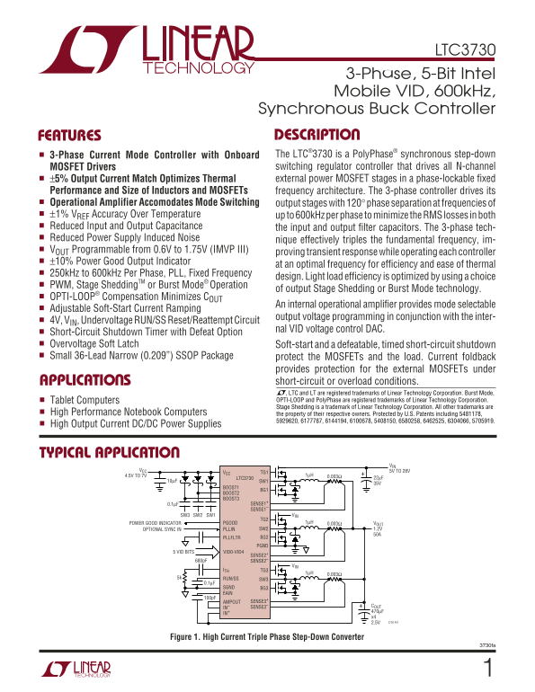
Figure 1. High Current Triple Phase Step-Down Converter

3730fa

Page Summary Contents For LINEAR TECHNOLOGY LTC3730 3-Phase, 5-Bit Intel Mobile VID, 600kHz, Synchronous Buck Controller User's Manual Data Sheet

Page 1 LTC3730 3-Phase, 5-Bit Intel Mobile VID, 600k Hz, Synchronous Buck Controller FEATURES DESCRIPTIO 3-Phase Current Mode Controller with Onboard The LTC®3730 is a Poly Phase® synchronous step-down MOSFE...
Page 2 LTC3730 ABSOLUTE AXI U RATI GS PACKAGE/ORDER I FOR ATIO (Note 1) Topside Driver Voltage (BOOSTN) Range 38V to –0.3V TOP VIEW ORDER PART Switch Voltage (SWN) Range........................ 32V to –5V VI...
Page 3 LTC3730 ELECTRICAL CHARACTERISTICS The ● denotes the specifications which apply over the full operating temperature range, otherwise specifications are at TA = 25°C. VCC = VRUN/SS = 5V unless otherwis...
Page 4 LTC3730 ELECTRICAL CHARACTERISTICS The ● denotes the specifications which apply over the full operating temperature range, otherwise specifications are at TA = 25°C. VCC = VRUN/SS = 5V unless otherwis...
Page 5 FR EQ UE NC (k Hz RE FE RE NC VO LT AG (m V) EF FI CI EN CY LTC3730 TYPICAL PERFOR A CE CHARACTERISTICS Efficiency vs IOUT (Figure 14) Efficiency vs VIN (Figure 14) Efficiency vs Frequency (Figure 14)...
Page 6 PE AK EN SE OL TA GE (m V) AX IM UM (m V) RU N/ SS IN OL TA GE (V EN SE LTC3730 TYPICAL PERFOR A CE CHARACTERISTICS Short-Circuit Arming and Latchoff RUN/SS Pull-Up Current vs vs Temperature Supply Cu...
Page 7 LTC3730 TYPICAL PERFOR A CE CHARACTERISTICS Operational Amplifier Gain-Phase GA IN (d B) PHASE (DEG) IN FREQUENCY (k Hz) Shed Mode at 1Amp, Light Load Burst Mode at 1Amp, Light Load Current (Circuit o...
Page 8 LTC3730 PI FU CTIO S VID0 to VID4 (Pins 1, 18, 19, 20, 36): Output Voltage RUN/SS (Pin 16): Combination of Soft-Start, Run Con- Programming Input Pins. A 3µA internal pull-up current is trol Input and...
Page 9 LTC3730 FU CTIO AL DIAGRA PLLIN FIN PHASE DET RLP PLLFLTR OSCILLATOR CLK2 CLK3 DUPLICATE FOR SECOND AND THIRD VCC VIN CONTROLLER CHANNELS BOOST FCB OUT 0.6V CB DET BOT TG FORCE BOT CIN PGOOD 0.66V SWI...
Page 10 LTC3730 OPERATIO (Refer to Functional Diagram) The top MOSFET drivers are biased from floating boot- results in output signals to the MOSFETs that turn them on strap capacitor CB, which is normally re...
Page 11 LTC3730 OPERATIO (Refer to Functional Diagram) aligns the turn on of the top MOSFET to the rising edge of Short-Circuit Detection the synchronizing signal. When no frequency information The RUN/SS cap...
Page 12 LTC3730 OS CI LL AT OR RE QU EN CY (k Hz APPLICATIO S I FOR ATIO The basic application circuit is shown in Figure 1 on the Inductor Value Calculation and Output Ripple Current first page of this data ...
Page 13 LTC3730 (P -P APPLICATIO S I FOR ATIO /f L Accepting larger values of ∆IL allows the use of low ferrite. A reasonable compromise from the same manu- inductances but can result in higher output voltage...
Page 14 LTC3730 APPLICATIO S I FOR ATIO drain-to-gate accumulation capacitance and the gate-to- where N is the number of output stages, δ is the tempera- source capacitance. The Miller charge (the increase in...
Page 15 LTC3730 APPLICATIO S I FOR ATIO RM IN PU RI PP LE UR RN ET DC OA CU RR EN rations with the output voltage fixed and input voltage of stages used. It is important to note that the efficiency varied. Th...
Page 16 LTC3730 APPLICATIO S I FOR ATIO COUT required ESR < N • RSENSE has a typical maximum threshold of 75m V/RSENSE and an input common mode range of SGND to (1.1) • VCC. The current comparator threshol...
Page 17 LTC3730 APPLICATIO S I FOR ATIO 30 to 100 times that of the total gate charge capacitance of Soft-Start/Run Function the topside MOSFET(s) as specified on the manufacturer’s The RUN/SS pin provides th...
Page 18 LTC3730 APPLICATIO S I FOR ATIO Fault Conditions: Overcurrent Latchoff protecting the power supply system from failure. A deci- sion can be made after the design is complete whether to The RUN/SS pins...
Page 19 LTC3730 APPLICATIO S I FOR ATIO Undervoltage Reset If the external frequency (f PLLIN) is greater than the oscil- lator frequency, f OSC, current is sourced continuously, In the event that the input p...
Page 20 LTC3730 APPLICATIO S I FOR ATIO The minimum on-time for the IC is generally about 110ns. second order system, phase margin and/or damping However, as the peak sense voltage decreases the mini- factor ...
Page 21 LTC3730 APPLICATIO S I FOR ATIO Automotive Considerations: Plugging into the voltage. Apply a 400k Hz signal into the PLLIN pin or apply Cigarette Lighter 1.2V to the PLLFLTR pin. As battery-powered d...
Page 22 LTC3730 APPLICATIO S I FOR ATIO The worst-case power dissipation by the synchronous der to keep the internal IC supply quiet. The power ground MOSFET under normal operating conditions at elevated retu...
Page 23 LTC3730 APPLICATIO S I FOR ATIO 7) Minimize trace impedances of TG, BG and SW nets. TG to the “noise” generated by a switching regulator. The and SW must be routed in parallel with minimum distance. g...
Page 24 LTC3730 APPLICATIO S I FOR ATIO Simplified Visual Explanation of How a 3-Phase The worst-case input RMS ripple current for a single stage Controller Reduces Both Input and Output RMS design peaks at t...
Page 25 LTC3730 APPLICATIO S I FOR ATIO Efficiency Calculation performance. A maximum operating junction temperature of 90° to 100°C for the MOSFETs is recommended for To estimate efficiency, the DC loss term...
Page 26 LTC3730 APPLICATIO S I FOR ATIO Total of all three synchronous MOSFETs’ AC gate loss: The total output power is (1.3V)(45A) = 58.5W and the total input power is approximately 60W so the % loss of IN I...
Page 27 LTC3730 PACKAGE DESCRIPTIO G Package 36-Lead Plastic SSOP (5.3mm) (Reference LTC DWG # 05-08-1640) 0.42 ±0.03 0.65 BSC RECOMMENDED SOLDER PAD LAYOUT BSC 0.05 NOTE: (.002) 1. CONTROLLING DIMENSION: MIL...
Page 28 LTC3730 ST PC PU TYPICAL APPLICATIO OPTIONAL FOR SYNCHRONIZATION ST PC PU PGOOD5V VID1 IN VID1 VID0 VID0 IN PLLIN PGOOD 5V PLLFLTR BOOST1 1Ω VIN 100p F 0.1µF VOUT FCB TG1 M1 L1 LTC3730 0.003Ω IN+ SW1 ...

Manual Details

Brand Linear
Pages 28
File Size 373.93 KB
Published June 21, 2026
10 views

Enter the captcha to get the download link:

captcha

Frequently Asked Questions

What is the maximum operating frequency per phase?

The controller supports operation up to 600kHz for each individual phase.

Does the LTC3730 provide protection against overcurrent or short circuits?

It includes a Short-Circuit Shutdown Timer and implements Current foldback to protect external MOSFETs under overload conditions.

What ambient temperature range is recommended for use?

The specified operating ambient temperature range is 0°C to 70°C.

How does the controller manage efficiency during light load conditions?

It uses Stage Shedding or Burst Mode technology along with OPTI-LOOP compensation to minimize power losses and optimize efficiency.

What is the programmable voltage control capability of the device?

The internal operational amplifier allows for Programmable VID (Voltage Identifier) from 0.6V to 1.75V using a DAC.