LINEAR TECHNOLOGY - 1 LTC1751 LTC1751-3.3 LTC1751-5 Data Sheet Owner's Manual
Summary
The LTC1751 family offers micropower, regulated charge pump DC/DC conversion solutions designed for ultra-low current battery applications. These converters reliably generate stable 3.3V or 5V outputs from input voltages ranging from 2V to 5.5V. The comprehensive manual details technical specifications, including efficiency curves, detailed operating parameters (such as soft-start and protection features), and practical application guidance. Ideal for engineers developing miniature electronics like smart card readers, LED backlighting systems, or portable battery backup supplies that require reliable, low-power voltage regulation.
Page 1 Text Content
LTC1751/LTC1751-3.3/LTC1751-5 Micropower, Regulated
Charge Pump DC/DC Converters
FEATURES DESCRIPTIO 5V Output Current: 100m A (VIN ≥ 3V) The LTC®1751 family are micropower charge pump DC/ 3.3V Output Current: 80m A (VIN ≥ 2.5V) DC converters that produce a regulated output voltage at Ultralow Power: 20µA Quiescent Current up to 100m A. The input voltage range is 2V to 5.5V. Regulated Output Voltage: 3.3V ±4%, 5V ±4%, ADJ Extremely low operating current (20µA typical with no No Inductors load) and low external parts count (one flying capacitor Short-Circuit/Thermal Protection and two small bypass capacitors at VIN and VOUT) make VIN Range: 2V to 5.5V them ideally suited for small, battery-powered applica- 800k Hz Switching Frequency tions. Very Low Shutdown Current: <2µA
The LTC1751 family operate as Burst Mode TM switched
Shutdown Disconnects Load from VIN
capacitor voltage doublers to achieve ultralow quiescent
Power Good/Undervoltage Output
current. They have thermal shutdown capability and can
Adjustable Soft-Start Time
survive a continuous short circuit from VOUT to GND. The
Available in an 8-Pin MSOP Package
PGOOD pin on the LTC1751-3.3 and LTC1751-5 indicates when the output voltage has reached its final value and if APPLICATIO S the output has an undervoltage fault condition. The FB pin OU TP UT OL TA GE (V of the adjustable LTC1751 can be used to program the
Li-Ion Battery Backup Supplies
desired output voltage or current. An optional soft-start
Local 3V and 5V Conversion
capacitor may be used at the SS pin to prevent excessive
Smart Card Readers
inrush current during start-up.
PCMCIA Local 5V Supplies
The LTC1751 family is available in an 8-pin MSOP
White LED Backlighting
package. , LTC and LT are registered trademarks of Linear Technology Corporation. Burst Mode is a trademark of Linear Technology Corporation.
TYPICAL APPLICATIO
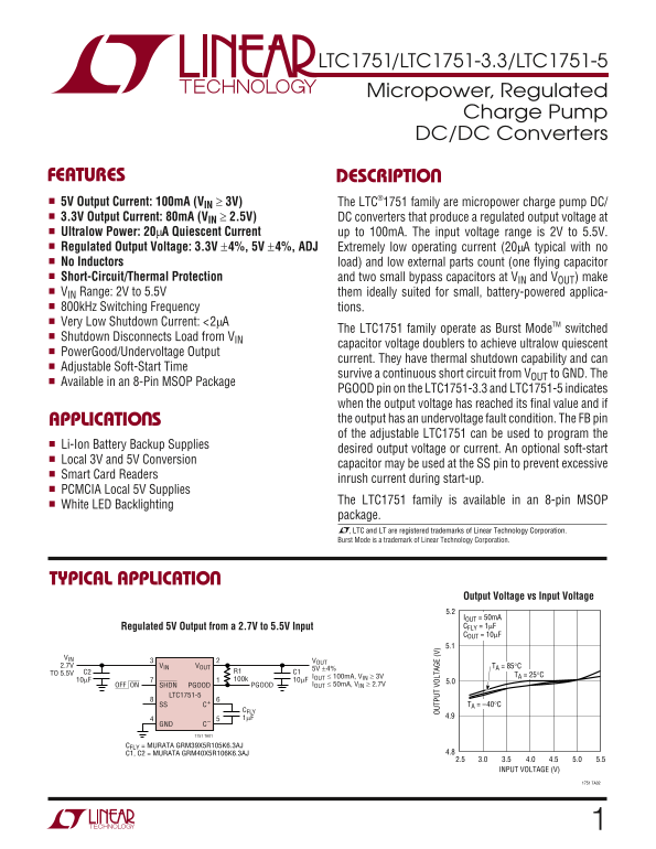
Output Voltage vs Input Voltage 5.2 IOUT = 50m A Regulated 5V Output from a 2.7V to 5.5V Input CFLY = 1µF COUT = 10µF 5.1
2.7V VIN VOUT TA = 85°C
TO 5.5V C2 R1 C1
IOUT ≤ 100m A, VIN ≥ 3V TA = 25°C
OFF ON SHDN PGOOD PGOOD IOUT ≤ 50m A, VIN ≥ 2.7V
LTC1751-5
SS C+ TA = –40°C
GND C–
1751 TA01
CFLY = MURATA GRM39X5R105K6.3AJ
C1, C2 = MURATA GRM40X5R106K6.3AJ 4.8 2.5 3.0 3.5 4.0 4.5 5.0 5.5
INPUT VOLTAGE (V)
1751 TA02
Page Summary Contents For LINEAR TECHNOLOGY - 1 LTC1751 LTC1751-3.3 LTC1751-5 Data Sheet Owner's Manual
Manual Details
| Brand | Linear |
|---|---|
| Pages | 12 |
| File Size | 209.32 KB |
| Published | June 18, 2026 |
Enter the captcha to get the download link:

Frequently Asked Questions
What input voltage range does the LTC1751 family support?
The system accepts an input voltage range from 2V to 5.5V.
How is output voltage monitored for faults?
The PGOOD pin on the LTC1751-3.3 and LTC1751-5 indicates when the output has reached its final value or if there is an undervoltage fault condition.
Can I use this converter with battery power?
Yes, it is described as ideally suited for small, battery-powered applications due to its features like low operating current and lack of inductors.
What happens during a short circuit?
The device provides Short-Circuit/Thermal Protection, allowing it to survive a continuous short circuit from V to GND indefinitely.