LINEAR LTC694-3.3 Data Sheet LTC695-3.3 Data Sheet
Summary
This advanced supervisory circuit, LTC694-3.3/LTC695-3.3, is designed for mission-critical 3.3V microprocessor systems requiring robust power management in low-power applications. It provides comprehensive protection features including power-on reset, battery backup capabilities, RAM write protection, and watchdog timing. The manual details its precision voltage monitoring (down to 1V) and ultra-low supply current (200μA typical), making it ideal for designers building smart instruments, intelligent controllers, or battery-powered industrial equipment where reliable system uptime is essential.
Page 1 Text Content
查询LTC694-3.3供应商
LTC694-3.3/LTC695-3.3 3.3V Microprocessor Supervisory Circuits
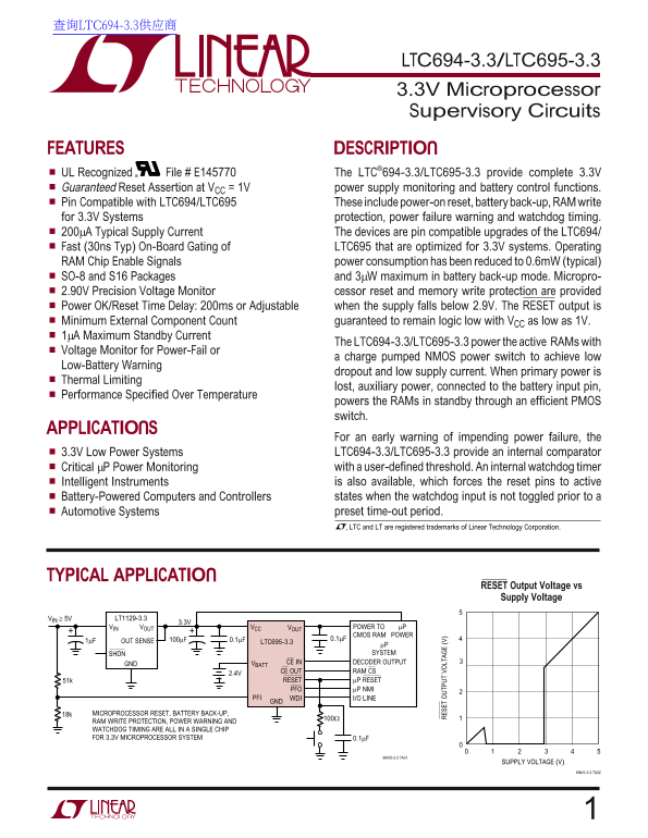
FEATURES DESCRIPTIO UL Recognized File # E145770 The LTC®694-3.3/LTC695-3.3 provide complete 3.3V Guaranteed Reset Assertion at VCC = 1V power supply monitoring and battery control functions. Pin Compatible with LTC694/LTC695 These include power-on reset, battery back-up, RAM write
for 3.3V Systems protection, power failure warning and watchdog timing. 200µA Typical Supply Current The devices are pin compatible upgrades of the LTC694/ Fast (30ns Typ) On-Board Gating of LTC695 that are optimized for 3.3V systems. Operating RAM Chip Enable Signals power consumption has been reduced to 0.6m W (typical) SO-8 and S16 Packages and 3µW maximum in battery back-up mode. Micropro- 2.90V Precision Voltage Monitor cessor reset and memory write protection are provided Power OK/Reset Time Delay: 200ms or Adjustable when the supply falls below 2.9V. The RESET output is Minimum External Component Count guaranteed to remain logic low with VCC as low as 1V.
1µA Maximum Standby Current
The LTC694-3.3/LTC695-3.3 power the active RAMs with
Voltage Monitor for Power-Fail or
a charge pumped NMOS power switch to achieve low
Low-Battery Warning
dropout and low supply current. When primary power is
Thermal Limiting
lost, auxiliary power, connected to the battery input pin,
Performance Specified Over Temperature
powers the RAMs in standby through an efficient PMOS switch.
APPLICATIO S
For an early warning of impending power failure, the
RE SE OU TP UT OL TA GE (V
3.3V Low Power Systems LTC694-3.3/LTC695-3.3 provide an internal comparator Critical µP Power Monitoring with a user-defined threshold. An internal watchdog timer Intelligent Instruments is also available, which forces the reset pins to active Battery-Powered Computers and Controllers states when the watchdog input is not toggled prior to a Automotive Systems preset time-out period. , LTC and LT are registered trademarks of Linear Technology Corporation.
TYPICAL APPLICATIO
RESET Output Voltage vs Supply Voltage
VIN ≥ 5V LT1129-3.3
VIN VOUT VOUTVCC POWER TO µP CMOS RAM POWER 1µF 100µF 0.1µF 0.1µF
OUT SENSE LTC695-3.3
µP SHDN SYSTEM
GND VBATT CE IN DECODER OUTPUT CE OUT RAM CS
51k RESET µP RESET PFO µP NMI
PFI WDI I/O LINE GND
18k MICROPROCESSOR RESET, BATTERY BACK-UP,
RAM WRITE PROTECTION, POWER WARNING AND WATCHDOG TIMING ARE ALL IN A SINGLE CHIP FOR 3.3V MICROPROCESSOR SYSTEM 0.1µF
694/5-3.3 TA01
SUPPLY VOLTAGE (V)
694/5-3.3 TA02
Page Summary Contents For LINEAR LTC694-3.3 Data Sheet LTC695-3.3 Data Sheet
Manual Details
| Brand | Linear |
|---|---|
| Pages | 16 |
| File Size | 142.89 KB |
| Published | June 03, 2026 |
Enter the captcha to get the download link:

Frequently Asked Questions
How does the device handle impending power failure events?
It provides low-battery warning dropout using an efficient PMOS switch or a charge pumped NMOS power switch.
What is the minimum voltage where critical signals are guaranteed to function?
The output is guaranteed to remain logic low even when the supply voltage drops as low as 1V.
How can I monitor for system failure in complex applications?
It offers an integrated watchdog timer, power warning features, and microprocessor reset capability in a single chip.
What are the typical current consumption levels of this module?
The typical supply current is 200µA, while the maximum standby current is only 1µA.