LINEAR TECHNOLOGY LTC690, LTC691, LTC694, LTC695 Data Sheet User Manual
Summary
The LTC 690 family supervisory circuit provides essential power monitoring and robust reset protection for embedded microprocessor systems. It acts as a system guardian, ensuring reliable operation by handling voltage undervoltage detection, guaranteed reset assertion at low voltages (down to 1V), and critical power-fail management using battery backup. This comprehensive guide details its technical specifications, advanced features like watchdog timing and RAM write protection, and diverse applications in automotive, industrial, and battery-powered controllers requiring utmost stability.
Page 1 Text Content
LTC690/LTC691 LTC694/LTC695 Microprocessor Supervisory Circuits
SFEATURE ESCRIPTIO
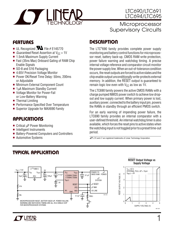
UL Recognized File # E145770 The LTC®690 family provides complete power supply Guaranteed Reset Assertion at VCC = 1V monitoring and battery control functions for microproces- 1.5m A Maximum Supply Current sor reset, battery back-up, CMOS RAM write protection, Fast (35ns Max) Onboard Gating of RAM Chip power failure warning and watchdog timing. A precise Enable Signals internal voltage reference and comparator circuit monitor SO-8 and S16 Packaging the power supply line. When an out-of-tolerance condition 4.65V Precision Voltage Monitor occurs, the reset outputs are forced to active states and the Power OK/Reset Time Delay: 50ms, 200ms chip enable output unconditionally write-protects external or Adjustable memory. In addition, the RESET output is guaranteed to Minimum External Component Count remain logic low even with VCC as low as 1V. 1µA Maximum Standby Current
The LTC690 family powers the active CMOS RAMs with a
Voltage Monitor for Power-Fail
charge pumped NMOS power switch to achieve low drop-
or Low-Battery Warning
out and low supply current. When primary power is lost,
Thermal Limiting
auxiliary power, connected to the battery input pin, powers
Performance Specified Over Temperature
the RAMs in standby through an efficient PMOS switch.
Superior Upgrade for MAX690 Family
For an early warning of impending power failure, the LTC690 family provides an internal comparator with a
PPLICATI RE SE OU TP UT SA OL TA GE (V user-defined threshold. An internal watchdog timer is also
available, which forces the reset pins to active states when
Critical µP Power Monitoring
the watchdog input is not toggled prior to a preset time-out
Intelligent Instruments
period.
Battery-Powered Computers and Controllers
Automotive Systems , LTC and LT are registered trademarks of Linear Technology Corporation.
PPLICATITYPICAL
RESET Output Voltage vs Supply Voltage
LT®1086-5 TA = 25°C
VIN ≥ 7.5V 5V
EXTERNAL PULL-UP = 10µA
VIN VOUT VOUTVCC POWER TO µP
VBATT = 0V
0.1µF CMOS RAM POWER LTC690/LTC691 0.1µF
10µF ADJ 100µF
LTC694/LTC695
VBATT SYSTEM 3V
RESET µP RESET
PFO µP NMI PFI WDI I/O LINE
10k 690 TA01
MICROPROCESSOR RESET, BATTERY BACK-UP, POWER FAILURE WARNING AND WATCHDOG TIMING ARE ALL IN A SINGLE CHIP FOR MICROPROCESSOR SYSTEMS
SUPPLY VOLTAGE (V)
690 TA02
Page Summary Contents For LINEAR TECHNOLOGY LTC690, LTC691, LTC694, LTC695 Data Sheet User Manual
Manual Details
| Brand | Linear |
|---|---|
| Pages | 16 |
| File Size | 223.25 KB |
| Published | May 29, 2026 |
Enter the captcha to get the download link:

Frequently Asked Questions
How does the LTC69x family handle imminent power failure?
The circuit provides a low-battery warning and maintains the RESET output guaranteed logic low even when voltage drops as low as 1V.
Can I use this device to detect processor stalls or freezes?
Yes, an integrated internal watchdog timer forces the reset pins active if its input is not toggled within a preset time period.
What temperature range does this monitoring circuit support?
The LTC690/LTC691 series typically operates from 0°C to 70°C, though other variants offer wide ranges like -55°C to 125°C.
Does implementation require many external components?
No. The design is noted for its minimum external component count, simplifying power-up and reset circuit integration.