# A B C D E F G H I J K L M N O P Q R S T U V W X Y Z

LINEAR TECHNOLOGY LT1794 Data Sheet Manual

Summary

This dual xDSL Line Driver Amplifier is an advanced component designed for high-density telecommunications applications, supporting ADSL, HDSL2, and G.lite architectures. It provides reliable 500mA output with outstanding low distortion performance, uniquely featuring extended output swing capability even when powered by lower supply rails—a key benefit for modern systems. This guide details the comprehensive electrical characteristics, absolute maximum ratings, and typical application circuits needed to successfully integrate this high-performance line driver into your central office equipment or cable plant technology.
📄 Preview PAGE OF 20

Page 1 Text Content

LT1794

Dual 500m A, 200MHz x DSL Line Driver Amplifier

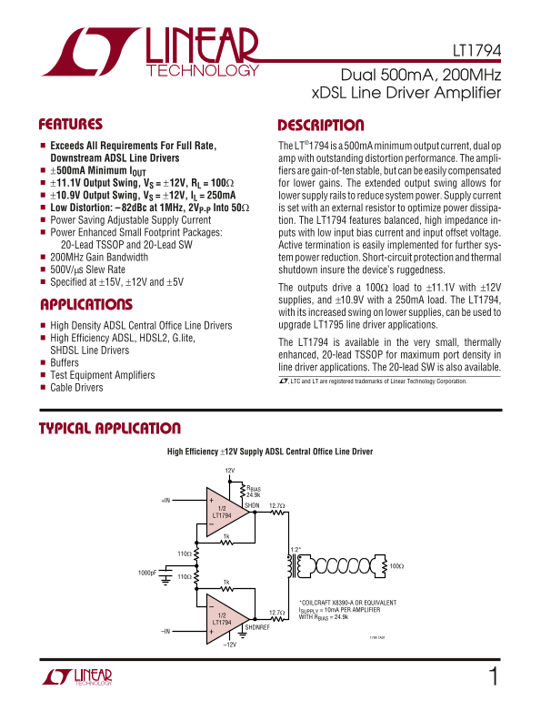
FEATURES DESCRIPTIO Exceeds All Requirements For Full Rate, The LT®1794 is a 500m A minimum output current, dual op Downstream ADSL Line Drivers amp with outstanding distortion performance. The ampli- ±500m A Minimum IOUT fiers are gain-of-ten stable, but can be easily compensated ±11.1V Output Swing, VS = ±12V, RL = 100Ω for lower gains. The extended output swing allows for ±10.9V Output Swing, VS = ±12V, IL = 250m A lower supply rails to reduce system power. Supply current Low Distortion: – 82d Bc at 1MHz, 2VP-P Into 50Ω is set with an external resistor to optimize power dissipa- Power Saving Adjustable Supply Current tion. The LT1794 features balanced, high impedance in- Power Enhanced Small Footprint Packages: puts with low input bias current and input offset voltage. 20-Lead TSSOP and 20-Lead SW Active termination is easily implemented for further sys- 200MHz Gain Bandwidth tem power reduction. Short-circuit protection and thermal 500V/µs Slew Rate shutdown insure the device’s ruggedness. Specified at ±15V, ±12V and ±5V

The outputs drive a 100Ω load to ±11.1V with ±12V supplies, and ±10.9V with a 250m A load. The LT1794,

APPLICATIO S

with its increased swing on lower supplies, can be used to High Density ADSL Central Office Line Drivers upgrade LT1795 line driver applications.

High Efficiency ADSL, HDSL2, G.lite,

The LT1794 is available in the very small, thermally

SHDSL Line Drivers

enhanced, 20-lead TSSOP for maximum port density in

Buffers

line driver applications. The 20-lead SW is also available.

Test Equipment Amplifiers

, LTC and LT are registered trademarks of Linear Technology Corporation.

Cable Drivers

TYPICAL APPLICATIO

High Efficiency ±12V Supply ADSL Central Office Line Driver

RBIAS 24.9k

SHDN 12.7Ω

1/2 LT1794

*COILCRAFT X8390-A OR EQUIVALENT ISUPPLY = 10m A PER AMPLIFIER

1/2 WITH RBIAS = 24.9k LT1794

SHDNREF

1794 TA01

Page Summary Contents For LINEAR TECHNOLOGY LT1794 Data Sheet Manual

Page 1 LT1794 Dual 500m A, 200MHz x DSL Line Driver Amplifier FEATURES DESCRIPTIO Exceeds All Requirements For Full Rate, The LT®1794 is a 500m A minimum output current, dual op Downstream ADSL Line Drivers ...
Page 2 LT1794 ABSOLUTE MAXIMUM RATINGS (Note 1) + to V –) Supply Voltage (V ±18V Specified Temperature Range (Note 3) 40°C to 85°C Input Current ±10m A Junction Temperature 150°C Output Short-Circuit Duratio...
Page 3 LT1794 ELECTRICAL CHARACTERISTICS The ● denotes the specifications which apply over the full specified temperature range, otherwise specifications are at TA = 25°C. + and SHDN unless otherwise noted. ...
Page 4 IN PU VO LT AG NO IS (V /V Hz UP PL PE AM PL IF IE (m A) LT1794 ELECTRICAL CHARACTERISTICS Note 1: Absolute Maximum Ratings are those values beyond which the life Note 4: Thermal resistance varies dep...
Page 5 OU TP UT IM PE DA NC (Ω CO ON OD RE JE CT IO RA TI (d B) GA IN (d B) LT1794 TYPICAL PERFOR A CE CHARACTERISTICS Open-Loop Gain and Phase –3d B Bandwidth vs Frequency vs Supply Current Slew Rate vs Sup...
Page 6 LT1794 DI ST OR TI ON (d Bc DI ST OR TI ON (d Bc TYPICAL PERFOR A CE CHARACTERISTICS Differential Harmonic Distortion Differential Harmonic Distortion vs Output Amplitude vs Frequency –40 –40 f = 1MHz...
Page 7 LT1794 TEST CIRCUIT SUPPLY BYPASSING RSHDN 10 (SHDN) VOUT(P-P) –12V 110ΩOUT (+) RL ≈ 50Ω EIN SPLITTER 100 LINE LOAD OUT (–) 110Ω MINICIRCUITS ZSC5-2-2 10k 1794 TC 11 (SHDNREF) *COILCRAFT X8390-A OR EQ...
Page 8 LT1794 APPLICATIO S I FOR ATIO SHDN outputs are in a high impedance state. Part to part varia- tions however, will cause inconsistent control of the qui- escent current if direct voltage drive of the ...
Page 9 LT1794 APPLICATIO S I FOR ATIO Logic Controlled Operating Current Shutdown and Recovery The DSP controller in a typical x DSL application can have The ultimate power saving action on a completely idle...
Page 10 LT1794 APPLICATIO S I FOR ATIO Power Dissipation and Heat Management Estimating Line Driver Power Dissipation x DSL applications require the line driver to dissipate a Figure 6 is a typical ADSL appli...
Page 11 LT1794 APPLICATIO S I FOR ATIO With no signal being placed on the line and the amplifier heat-spreading PCB metal and airflow through the enclo- biased for 10m A per amplifier supply current, the quie...
Page 12 LT1794 APPLICATIO S I FOR ATIO Figure 8 shows four examples of PCB metal being used for board produces a thermal resistance from junction to heat spreading. These are provided as a reference for what ...
Page 13 LT1794 APPLICATIO S I FOR ATIO Similar results can be obtained with the LT1794CSW in the Figure␣ 9 shows that for inverting gains, a resistor from the wide SO-20 package. With this package heat is con...
Page 14 LT1794 APPLICATIO S I FOR ATIO CABLE OR LINE WITH CHARACTERISTIC IMPEDANCE RL RC VO RF = 1 AT LOW FREQUENCIES VI RF RF RBT = RL = 1 + AT MEDIUM FREQUENCIES RG VO (1 + RF/RG) = VI CBIG RF = 1 + AT HIGH...
Page 15 LT1794 APPLICATIO S I FOR ATIO Note that the overall gain is increased: Figure 17 shows a full-rate ADSL line driver incorporating positive feedback to reduce the power lost in the back termination re...
Page 16 LT1794 APPLICATIO S I FOR ATIO Using DC blocking capacitors, as shown in Figure 16, to create fast voltage transitions themselves that can be AC couple the signal to the transformer eliminates the cou...
Page 17 LT1794 SI PLIFIED SCHE ATIC (one amplifier shown) –IN Q6 +IN OUTQ2 Q15 C2 1794 SS
Page 18 LT1794 PACKAGE DESCRIPTIO Dimensions in inches (millimeters) unless otherwise noted. FE Package 20-Lead Plastic TSSOP (4.4mm) (Reference LTC DWG # 05-08-1663) Exposed Pad Variation CA SEE NOTE 4 (.108...
Page 19 LT1794 PACKAGE DESCRIPTIO Dimensions in inches (millimeters) unless otherwise noted. SW Package 20-Lead Plastic Small Outline (Wide 0.300) (LTC DWG # 05-08-1620) NOTE 1 0.394 – 0.419 (10.007 – 10.643)...
Page 20 LT1794 TYPICAL APPLICATIO SHDN 13.7Ω 1/2 LT1794 *COILCRAFT X8502-A OR EQUIVALENT 1W DRIVER POWER DISSIPATION 1.15W POWER CONSUMPTION LT1794 SHDNREF Figure 17. ADSL Line Driver Using Active Termination...

Manual Details

Brand Linear
Pages 20
File Size 275.52 KB
Published May 25, 2026
139 views

Enter the captcha to get the download link:

captcha

Frequently Asked Questions

What is the minimum output current and maximum gain bandwidth?

The device features a 500mA minimum output current and offers a 200MHz gain bandwidth.

How can I improve power efficiency while maintaining output capabilities?

The LT1794 supports adjustable supply current and includes an extended output swing, allowing operation on lower supply rails to reduce system power.

What is the maximum operating temperature range for this line driver amplifier?

Its specified temperature range is –40°C to 85°C, with a junction temperature limit of 150°C.

Does the device offer features to ensure reliable use in commercial settings?

Yes, it includes short-circuit protection and thermal shutdown, ensuring the device's ruggedness for applications like ADSL Central Office Line Drivers.