# A B C D E F G H I J K L M N O P Q R S T U V W X Y Z

LINEAR TECHNOLOGY LT3480 Data Sheet

Summary

This technical manual details the LT3480, a high-efficiency, adjustable frequency monolithic buck switching regulator. It is designed to maintain stable power for critical systems requiring wide input voltage support and exceptional efficiency across various loads. The document provides detailed specifications on advanced features such as Burst Mode operation, soft-start capability, Power Good flagging, and ultra-low shutdown current (<1µA). Ideal for engineers designing portable electronics, automotive battery regulation systems, and complex distributed industrial power supplies.
📄 Preview PAGE OF 24

Page 1 Text Content

LT3480

36V, 2A, 2.4MHz Step-Down Switching Regulator with 70µA Quiescent Current

FEATURES DESCRIPTION n Wide Input Range:

The LT®3480 is an adjustable frequency (200k Hz to

Operation from 3.6V to 36V 2.4MHz) monolithic buck switching regulator that ac- Over-Voltage Lockout Protects Circuits cepts input voltages up to 36V (60V maximum). A high through 60V Transients effi ciency 0.25 switch is included on the die along with n 2A Maximum Output Current

a boost Schottky diode and the necessary oscillator, con-

n Low Ripple Burst Mode® Operation

trol, and logic circuitry. Current mode topology is used

70μA IQ at 12VIN to 3.3VOUT for fast transient response and good loop stability. Low Output Ripple < 15m V ripple Burst Mode operation maintains high effi ciency at n Adjustable Switching Frequency: 200k Hz to 2.4MHz

low output currents while keeping output ripple below

n Low Shutdown Current: IQ < 1μA

15m V in a typical application. In addition, the LT3480 can

n Integrated Boost Diode

further enhance low output current effi ciency by draw-

n Synchronizable Between 250k Hz to 2MHz

ing bias current from the output when VOUT is above 3V.

n Power Good Flag

Shutdown reduces input supply current to less than 1μA

n Saturating Switch Design: 0.25 On-Resistance

while a resistor and capacitor on the RUN/SS pin provide a

n 0.790V Feedback Reference Voltage

controlled output voltage ramp (soft-start). A power good

n Output Voltage: 0.79V to 20V

fl ag signals when VOUT reaches 86% of the programmed

FF IC IE

n Soft-Start Capability

output voltage. The LT3480 is available in 10-Pin MSOP

n Small 10-Pin Thermally Enhanced MSOP and

and 3mm × 3mm DFN packages with exposed pads for

(3mm × 3mm) DFN Packages low thermal resistance.

, LT, LTC and LTM are registered trademarks of Linear Technology Corporation.

APPLICATIONS

Burst Mode is a registered trademark of Linear Technology Corporation. All other trademarks are the property of their respective owners.

n Automotive Battery Regulation

n Power for Portable Products

n Distributed Supply Regulation

n Industrial Supplies

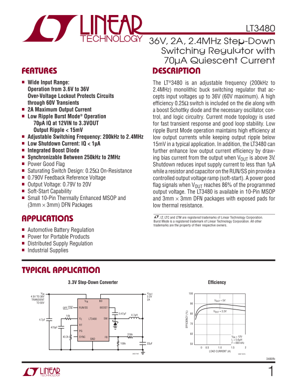
TYPICAL APPLICATION

3.3V Step-Down Converter Effi ciency

VIN VOUT

4.5V TO 36V 3.3V TRANSIENT 2A VOUT = 5V

VIN BD

TO 60V

OFF ON RUN/SS BOOST

VOUT = 3.3V

VC LT3480 SW

40.2k SYNC FB VIN = 12V

GND L = 5.6μH

22μF100k F = 800 k Hz

0.5 1.0 1.5 LOAD CURRENT (A)

3480 TA01 3480 TA01b

3480fb

Page Summary Contents For LINEAR TECHNOLOGY LT3480 Data Sheet

Page 1 LT3480 36V, 2A, 2.4MHz Step-Down Switching Regulator with 70µA Quiescent Current FEATURES DESCRIPTION n Wide Input Range: The LT®3480 is an adjustable frequency (200k Hz to Operation from 3.6V to 36V ...
Page 2 LT3480 ABSOLUTE MAXIMUM RATINGS (Note 1) VIN, RUN/SS Voltage (Note 5) ...................................60V Operating Temperature Range (Note 2) BOOST Pin Voltage .......................................
Page 3 LT3480 ELECTRICAL CHARACTERISTICS The l denotes the specifi cations which apply over the full operating temperature range, otherwise specifi cations are at TA = 25°C. VIN = 10V, VRUN/SS = 10V, VBOOST ...
Page 4 LY FF IC IE LT3480 TYPICAL PERFORMANCE CHARACTERISTICS Effi ciency Effi ciency Effi ciency VIN = 7V VIN = 12V VIN = 12V VIN = 34V VIN = 34V VIN = 24V VIN = 24V FF IC IE IT IM IT (A LY VIN = 12V VOUT =...
Page 5 IT IM IT FR z) LT LT3480 TYPICAL PERFORMANCE CHARACTERISTICS Switch Voltage Drop Boost Pin Current Feedback Voltage /S IN IT IN k H z) IN SWITCH CURRENT (m A) SWITCH CURRENT (m A) TEMPERATURE (°C) Swi...
Page 6 LT3480 TYPICAL PERFORMANCE CHARACTERISTICS Error Amp Output Current Minimum Input Voltage Minimum Input Voltage –10 5.0 IN LT VOUT = 3.3V VOUT = 5V –30 4.5 TA = 25 °C 2.5 TA = 25°C f = 800k Hz f = 800...
Page 7 LT3480 PIN FUNCTIONS BD (Pin 1): This pin connects to the anode of the boost SYNC (Pin 6): This is the external clock synchronization Schottky diode. BD also supplies current to the internal input. Gr...
Page 8 LT3480 OPERATION The LT3480 is a constant frequency, current mode step- The switch driver operates from either the input or from down regulator. An oscillator, with frequency set by RT, the BOOST pin....
Page 9 LT3480 APPLICATIONS INFORMATION FB Resistor Network where VIN is the typical input voltage, VOUT is the output voltage, VD is the catch diode drop (~0.5V) and VSW is the The output voltage is programm...
Page 10 LT3480 APPLICATIONS INFORMATION frequency. A reasonable starting point for selecting the –= VIN ripple current is: MAX SW( SW ON MIN ΔIL = 0.4(IOUT(MAX)) where VIN(MAX) is the maximum operating input ...
Page 11 LT3480 APPLICATIONS INFORMATION Table 1. Inductor Vendors necessary. This can be provided with a lower performance VENDOR URL PART SERIES TYPE electrolytic capacitor. Murata www.murata.com LQH55D Open...
Page 12 LT3480 APPLICATIONS INFORMATION Table 2. Capacitor Vendors VENDOR PHONE URL PART SERIES COMMANDS Panasonic (714) 373-7366 www.panasonic.com Ceramic, Polymer, EEF Series Tantalum Kemet (864) 963-6300 w...
Page 13 LT3480 APPLICATIONS INFORMATION operation, the noise is typically very quiet to a casual ear. current proportional to the voltage at the VC pin. Note that If this is unacceptable, use a high performan...
Page 14 LT3480 APPLICATIONS INFORMATION operation at a lower output load current than when in Burst Mode. The front page application circuit will switch at full frequency at output loads higher than about 60m...
Page 15 LT3480 APPLICATIONS INFORMATION VOUT 6.0 BD 5.5 TO START BOOST (WORST CASE) VIN VIN LT3480 C3 SW 4.7μF GND 4.0 TO RUN 3.5 3.0 VOUT = 3.3V TA = 25°C (5a) For VOUT &gt; 2.8V 2.5 L = 8.2μH f = 700k Hz 2....
Page 16 LT3480 APPLICATIONS INFORMATION D4 MBRS140 IL VIN VIN BOOST RUN 1A/DI LT3480 RUN/SS SW VOUT RUN/SS VRUN/ 2V/DI VC 0.22μF GND GND FB VOUT 2V/DI BACKUP 2ms/DIV 3480 F07 Figure 7. To Soft-Start the LT348...
Page 17 LT3480 APPLICATIONS INFORMATION Finally, keep the FB and VC nodes small so that the ground traces will shield them from the SW and BOOST nodes. The Exposed Pad on the bottom of the package must be sol...
Page 18 LT3480 APPLICATIONS INFORMATION source, forms an under damped tank circuit, and the the thermal resistance from die (or junction) to ambient can voltage at the VIN pin of the LT3480 can ring to twice ...
Page 19 LT3480 TYPICAL APPLICATIONS 3.3V Step-Down Converter VIN VOUT 4.4V TO 36V 3.3V TRANSIENT VIN BD 2A TO 60V* ON OFF RUN/SS BOOST VC SW LT3480 40.2k SYNC f = 800k Hz 3480 TA03 D: DIODES INC. DFLS240L L: ...
Page 20 LT3480 TYPICAL APPLICATIONS 5V, 2MHz Step-Down Converter VIN VOUT 8.6V TO 22V 5V TRANSIENT TO 38V VIN BD 2A ON OFF RUN/SS BOOST VC SW LT3480 11.5k SYNC FB GND f = 2MHz 3480 TA05 D: DIODES INC. DFLS240...
Page 21 LT3480 TYPICAL APPLICATIONS 1.8V Step-Down Converter VIN VOUT 3.5V TO 27V 1.8V VIN BD 2A ON OFF RUN/SS BOOST VC SW LT3480 68.1k SYNC FB f = 500k Hz 3480 TA08 D: DIODES INC. DFLS240L L: TAIYO YUDEN NP0...
Page 22 LT3480 PACKAGE DESCRIPTION DD Package 10-Lead Plastic DFN (3mm × 3mm) (Reference LTC DWG # 05-08-1660) 0.05 (2 SIDES)2.15 (4 SIDES) (2 SIDES) PIN 1 PACKAGE TOP MARK OUTLINE (SEE NOTE 6) (DD) DFN 1103 ...
Page 23 LT3480 PACKAGE DESCRIPTION MSE Package 10-Lead Plastic MSOP (Reference LTC DWG # 05-08-1660) BOTTOM VIEW OF EXPOSED PAD OPTION TYP BSC (NOTE 3) RECOMMENDED SOLDER PAD LAYOUT (NOTE 4) DETAIL “A” – 6 TY...
Page 24 LT3480 TYPICAL APPLICATION 1.2V Step-Down Converter VIN VOUT 3.6V TO 27V 1.2V VIN BD 2A ON OFF RUN/SS BOOST VC SW LT3480 68.1k FB f = 500k Hz 3480 TA09 D: DIODES INC. DFLS240L L: TAIYO YUDEN NP06DZB3R...

Manual Details

Brand Linear
Pages 24
File Size 304.86 KB
Published May 25, 2026
169 views

Enter the captcha to get the download link:

captcha

Frequently Asked Questions

What is the operating input voltage range for this regulator?

It accepts input voltages from 3.6V up to 36V (with a 60V absolute maximum).

How does it maintain efficiency during low output currents?

It features integrated boost diode and Burst Mode operation, allowing efficient draw-down of bias current while maintaining low output ripple.

Can I configure the startup voltage ramp?

Yes, it includes a soft-start capability controlled by an external resistor and capacitor on the RUN/SS pin to ramp the output voltage from 0.79V to 20V.

What are the package options for the LT3480?

It is available in 10-Pin MSOP, 16-Pin QSOP, and specific 3mm × 3mm DFN packages.