# A B C D E F G H I J K L M N O P Q R S T U V W X Y Z

LINEAR TECHNOLOGY LT3150 Data Sheet

Summary

This advanced linear regulator controller provides fast transient response and ultra-low dropout voltage, optimizing power delivery for sensitive electronics. It features an integrated fixed frequency boost converter and LDO output sequencing control, allowing precise management of multiple power rails. Optimized with high-side current limit protection and configurable shutdown pins, this device is essential for engineers designing microprocessor, ASIC, or complex I/O supply systems needing highly stable, low-voltage power conversion.
📄 Preview PAGE OF 20

Page 1 Text Content

LT3150

Fast Transient Response,

Low Input Voltage, Very Low Dropout

Linear Regulator Controller

FEATURES DESCRIPTIO Fast Transient Response Optimized with The LT®3150 drives a low cost external N-channel MOSFET Ceramic Output Capacitors as a source follower to produce a fast transient response, FET RDS(ON) Defines Dropout Voltage very low dropout voltage linear regulator. Selection of the ±1% Reference Tolerance Over Temperature N-channel MOSFET RDS(ON) allows dropout voltages below Multifunction LDO Shutdown Pin with Latchoff 300m V for low VIN to low VOUT applications. Fixed Frequency 1.4MHz Boost Converter Generates

The LT3150 includes a fixed frequency boost regulator

MOSFET Gate Drive

that generates gate drive for the N-channel MOSFET. The

Internally Compensated Boost Converter Uses Tiny

internally compensated current mode PWM architecture

Capacitors and Inductor

combined with the 1.4MHz switching frequency permits

Independent Boost Converter Shutdown Control

the use of tiny, low cost capacitors and inductors.

Permits LDO Output Voltage Supply Sequencing

16-Lead SSOP Package The LT3150’s transient load performance is optimized with ceramic output capacitors. A precision 1.21V refer- ence accommodates low voltage supplies.

APPLICATIO S

Protection includes a high side current limit amplifier that

Microprocessor, ASIC and I/O Supplies activates a fault timer circuit. A multifunction shutdown Very Low Dropout Input-to-Output Conversion pin provides either current limit time-out with latchoff, Logic Termination Supplies overvoltage protection or thermal shutdown. Independent , LTC and LT are registered trademarks of Linear Technology Corporation. shutdown control of the boost converter provides on/off

and sequencing control of the LDO output voltage.

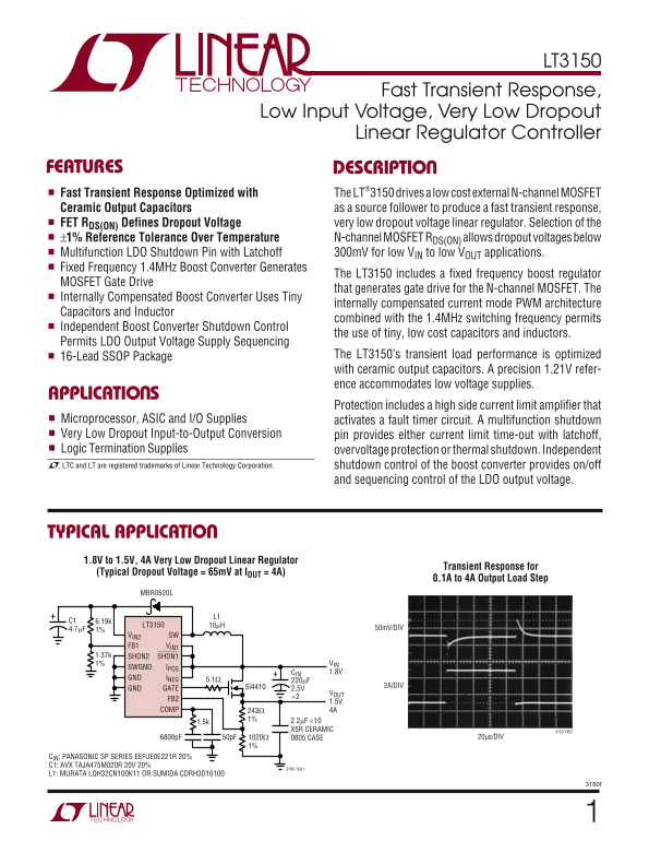
TYPICAL APPLICATIO 1.8V to 1.5V, 4A Very Low Dropout Linear Regulator

Transient Response for

(Typical Dropout Voltage = 65m V at IOUT = 4A)

0.1A to 4A Output Load Step

MBR0520L

LT3150 10µH

4.7µF 50m V/DIV

VIN2 SW FB1 VIN1

1.37k SHDN2 SHDN1

1% VIN

SWGND IPOS

CIN 1.8V

GND INEG 5.1Ω

Si4410 2A/DIV

GND GATE 2.5V

COMP 243Ω 4A

X5R CERAMIC 3150 TA02

6800p F 50p F 1020Ω 0805 CASE 20µs/DIV

CIN: PANASONIC SP SERIES EEFUE0E221R 20% C1: AVX TAJA475M020R 20V 20%

3150 TA01

L1: MURATA LQH32CN100K11 OR SUMIDA CDRH3D16100

Page Summary Contents For LINEAR TECHNOLOGY LT3150 Data Sheet

Page 1 LT3150 Fast Transient Response, Low Input Voltage, Very Low Dropout Linear Regulator Controller FEATURES DESCRIPTIO Fast Transient Response Optimized with The LT®3150 drives a low cost external N-chan...
Page 2 LT3150 ABSOLUTE AXI U RATI GS PACKAGE/ORDER I FOR ATIO (Note 1) VIN1, SHDN1 Voltage 10V TOP VIEW ORDER PART SW Voltage –0.4V to 36V NUMBER SW FB1 FB1 Voltage VIN1 + 0.3V SWGND GND LT3150CGN Current in...
Page 3 LT3150 ELECTRICAL CHARACTERISTICS The ● denotes specifications which apply over the full operating temperature range, otherwise specifications are at TA = 25°C. VIN1 = 1.5V, VSHDN1 = VIN1, VIN2 = 12V,...
Page 4 ES AT (m V) N2 UI ES CE NT UR RE NT (m A) LT3150 TYPICAL PERFOR A CE CHARACTERISTICS Boost Switching Regulator Oscillator Frequency SHDN1 Input Bias Current SW IT CH UR RE NT IM IT (m A) Switch VCESAT...
Page 5 FB LI NE EG UL AT IO /V CU RR EN LI IT HR ES HO LD OL TA GE (m V) GA TE UT PU SW IN LO (V LT3150 TYPICAL PERFOR A CE CHARACTERISTICS Linear Regulator Controller FB2 Line Regulation Error Amplifier Lar...
Page 6 LT3150 TYPICAL PERFOR A CE CHARACTERISTICS Linear Regulator Controller SH DN HI GH LA VO LT AG (V SH DN SO UR CE UR RE NT (µ A) SHDN2 Source Current SHDN2 Low Clamp Voltage vs Temperature vs Temperatu...
Page 7 LT3150 PI FU CTIO S VIN2 (Pin 5): This is the input supply for the linear regulator INEG (Pin 12): This is the negative sense terminal of the control circuitry and provides sufficient gate drive compl...
Page 8 LT3150 BLOCK DIAGRA S Boost Switching Regulator VIN1VIN1 R5 R6 40k 40k gm = 77µmhos VIN2 SW COMPARATOR A1 DRIVER (EXTERNAL) FF Q2 ΣRAMP FB1 GENERATOR x10 CC ILIM1 0.15Ω (EXTERNAL) 30k 1.4MHz OSCILLATO...
Page 9 LT3150 APPLICATIO S I FOR ATIO INTRODUCTION The LT3150 controller IC is a unique, easy-to-use device that drives an external N-channel MOSFET as a source With each new generation of computing systems,...
Page 10 LT3150 APPLICATIO S I FOR ATIO is low enough such that Q1 and Q2 do not saturate, even the COMP pin. The output impedance of the gm stage is when VIN1 is 1V. When there is no load, FB1 rises slightly ...
Page 11 LT3150 APPLICATIO S I FOR ATIO solutions for microprocessor power supplies. This signifi- 1µF capacitor on the SHDN2 pin yields a 74ms ramp time. cant performance benefit is what permits the eliminati...
Page 12 LT3150 APPLICATIO S I FOR ATIO holds internal comparator COMP3’s output low. This BOOST REGULATOR COMPONENT SELECTION comparator circuit, now enabled, monitors the GATE pin and detects saturation at t...
Page 13 LT3150 APPLICATIO S I FOR ATIO Table 1. Inductor Vendors VENDOR PHONE URL PART NUMBER INDUCTANCE DCR ISAT Murata (404) 436-1300 www.murata.com LQH31CN100K03K 10µH 1.3Ω 0.23A LQH32CN100K23K 10µH 0.44Ω ...
Page 14 LT3150 CH AN GE IN AL UE APPLICATIO S I FOR ATIO Figures 1 and 2 show voltage coefficient and temperature tics. Although the factor of three is slightly conservative, coefficient comparisons between Y...
Page 15 LT3150 APPLICATIO S I FOR ATIO Frequency Compensation Refer to the simplified LT3150 block diagram shown in Figure 3 during the frequency compensation discussion Frequency compensation is the most cri...
Page 16 LT3150 GA IN (d B) APPLICATIO S I FOR ATIO P1 = 1/(2 • π • RO • C1) P1 = 1/(2 • π • RO • C1) AVOL = gm1 • RO • (VREF/VOUT) AVOL = gm1 • RO • (VREF/VOUT) P2 IS A FUNCTION P2 IS A FUNCTION Z1 = 1/(2 • π...
Page 17 LT3150 TYPICAL APPLICATIO S Setting the Linear Regulator Output Voltage Using No RSENSE Current Limit VOUT D1 MBR0520L IPOSSHDN2 VIN1 FB2 10µF GATE Q1 VOUT = 1.21V(1 + R2/R1) 3150 TA03 3150 TA04VOUT S...
Page 18 LT3150 TYPICAL APPLICATIO S 1.5V to 1.2V, 4A Very Low Dropout Linear Regulator MBR0520L LT3150 10µH VIN2 SW FB1 VIN1 SHDN2 SHDN1 1% SWGND IPOS GND INEG 5.1Ω GND GATE Si4410 FB2 ×2 VOUT COMP 1.2V 4A X5...
Page 19 LT3150 PACKAGE DESCRIPTIO GN Package 16-Lead Plastic SSOP (Narrow .150 Inch) (Reference LTC DWG # 05-08-1641) .009 (0.229) REF .254 MIN .150 – .165 .0015 .0250 TYP.0165 ± RECOMMENDED SOLDER PAD LAYOUT...
Page 20 LT3150 TYPICAL APPLICATIO 1.8V to 1.5V, 4A Very Low Dropout Linear Regulator with No RSENSE Current Limiting and Shutdown MBR0520L LT3150 VIN2 SW FB1 VIN1 10k SHDN1 1.37k SHDN2 SHDN2 SHDN1 1% SWGND IP...

Manual Details

Brand Linear
Pages 20
File Size 253.86 KB
Published June 06, 2026
48 views

Enter the captcha to get the download link:

captcha

Frequently Asked Questions

What is the typical dropout voltage under heavy load?

The liquid regulator has a typical dropout voltage of 65mV when operating at 4A.

How can I control startup and shutdown sequencing?

It features independent boost converter shutdown control, allowing on/off and sequencing control of the LDO output voltage.

What are the specified ambient temperature limits?

The recommended operating ambient temperature range is from 0°C to 70°C.

Is this regulator suitable for low-voltage supplies?

Yes, it accommodates low voltage supplies with a precision 1.21V reference and requires a minimum operating voltage of 0.9V.