LINEAR TECHNOLOGY - LT6552 Data Sheet
Summary
This versatile high-speed video difference amplifier is optimized for driving signals in demanding applications, including automotive displays and general video line interfaces. Featuring rail-to-rail output, a wide operating voltage range (3V to 12.6V), and robust differential input support, it provides high bandwidth performance up to 75MHz at -3dB. The manual details technical specifications for implementing single/differential conversion, low-power operation, and driving coaxial cables directly, making it essential for engineers requiring reliable signal integrity in professional electronics design.
Page 1 Text Content
LT6552
3.3V Single Supply
Video Difference Amplifier
FEATURES DESCRIPTIO
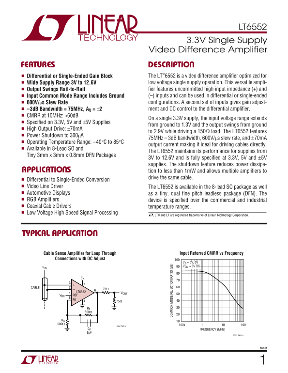
Differential or Single-Ended Gain Block The LT®6552 is a video difference amplifier optimized for Wide Supply Range 3V to 12.6V low voltage single supply operation. This versatile ampli- Output Swings Rail-to-Rail fier features uncommitted high input impedance (+) and Input Common Mode Range Includes Ground (–) inputs and can be used in differential or single-ended 600V/µs Slew Rate configurations. A second set of inputs gives gain adjust- –3d B Bandwidth = 75MHz, AV = ±2 ment and DC control to the differential amplifier.
CMRR at 10MHz: >60d B
On a single 3.3V supply, the input voltage range extends
Specified on 3.3V, 5V and ±5V Supplies
from ground to 1.3V and the output swings from ground
High Output Drive: ±70m A
to 2.9V while driving a 150Ω load. The LT6552 features
Power Shutdown to 300µA
75MHz – 3d B bandwidth, 600V/µs slew rate, and ±70m A
Operating Temperature Range: –40°C to 85°C
output current making it ideal for driving cables directly.
Available in 8-Lead SO and
The LT6552 maintains its performance for supplies from
Tiny 3mm x 3mm x 0.8mm DFN Packages
3V to 12.6V and is fully specified at 3.3V, 5V and ±5V supplies. The shutdown feature reduces power dissipa-
APPLICATIO S CO ON OD RE JE CT IO RA TI (d B) tion to less than 1m W and allows multiple amplifiers to
drive the same cable.
Differential to Single-Ended Conversion Video Line Driver The LT6552 is available in the 8-lead SO package as well Automotive Displays as a tiny, dual fine pitch leadless package (DFN). The RGB Amplifiers device is specified over the commercial and industrial Coaxial Cable Drivers temperature ranges. Low Voltage High Speed Signal Processing
, LTC and LT are registered trademarks of Linear Technology Corporation.
TYPICAL APPLICATIO
Input Referred CMRR vs Frequency Cable Sense Amplifier for Loop Through
Connections with DC Adjust
VS = 5V, 0V VCM = 0V DC
CABLE
75Ω 6LT6552
VDC REF FB
RF 500Ω
RG 500Ω 100k
6552 TA01a
CF FREQUENCY (MHz) 8p F
6552 TA01b
Page Summary Contents For LINEAR TECHNOLOGY - LT6552 Data Sheet
Manual Details
| Brand | Linear |
|---|---|
| Pages | 16 |
| File Size | 350.32 KB |
| Published | May 29, 2026 |
Enter the captcha to get the download link:

Frequently Asked Questions
What is the recommended operating temperature range for the LT6552?
The specified operating temperature range is –40°C to 85°C.
How many different package types are available for this device?
It is available in 8-Lead SO and a tiny dual fine pitch leadless DFN package.
What is the maximum output current when driving a 150Ω load?
The high output drive capability is up to ±70mA to 2.9V while driving a 150Ω load.
Can this amplifier be used in differential or single-ended configurations?
Yes, it is versatile and can be used in both differential or single-ended input configurations.