# A B C D E F G H I J K L M N O P Q R S T U V W X Y Z

LINEAR TECHNOLOGY LT6552 User's Manual

Summary

The LT6552 is a high-speed Video Difference Amplifier designed for robust low-voltage single or differential supply video signal processing. Featuring wide rail-to-rail output swings, excellent CMRR, and optimized performance from 3V to 12.6V, it ensures reliable operation in demanding environments like automotive displays. This manual provides comprehensive technical details, application examples, and rigorous specifications covering electrical characteristics for various supplies and temperature ranges, making it ideal for engineers building high-performance video line drivers and signal conditioners.
📄 Preview PAGE OF 16

Page 1 Text Content

LT6552

3.3V Single Supply

Video Difference Amplifier

FEATURES DESCRIPTIO

Differential or Single-Ended Gain Block The LT®6552 is a video difference amplifier optimized for Wide Supply Range 3V to 12.6V low voltage single supply operation. This versatile ampli- Output Swings Rail-to-Rail fier features uncommitted high input impedance (+) and Input Common Mode Range Includes Ground (–) inputs and can be used in differential or single-ended 600V/µs Slew Rate configurations. A second set of inputs gives gain adjust- –3d B Bandwidth = 75MHz, AV = ±2 ment and DC control to the differential amplifier.

CMRR at 10MHz: >60d B

On a single 3.3V supply, the input voltage range extends

Specified on 3.3V, 5V and ±5V Supplies

from ground to 1.3V and the output swings from ground

High Output Drive: ±70m A

to 2.9V while driving a 150Ω load. The LT6552 features

Power Shutdown to 300µA

75MHz – 3d B bandwidth, 600V/µs slew rate, and ±70m A

Operating Temperature Range: –40°C to 85°C

output current making it ideal for driving cables directly.

Available in 8-Lead SO and

The LT6552 maintains its performance for supplies from

Tiny 3mm x 3mm x 0.8mm DFN Packages

3V to 12.6V and is fully specified at 3.3V, 5V and ±5V supplies. The shutdown feature reduces power dissipa-

APPLICATIO S CO ON OD RE JE CT IO RA TI (d B) tion to less than 1m W and allows multiple amplifiers to

drive the same cable.

Differential to Single-Ended Conversion Video Line Driver The LT6552 is available in the 8-lead SO package as well Automotive Displays as a tiny, dual fine pitch leadless package (DFN). The RGB Amplifiers device is specified over the commercial and industrial Coaxial Cable Drivers temperature ranges. Low Voltage High Speed Signal Processing

, LTC and LT are registered trademarks of Linear Technology Corporation.

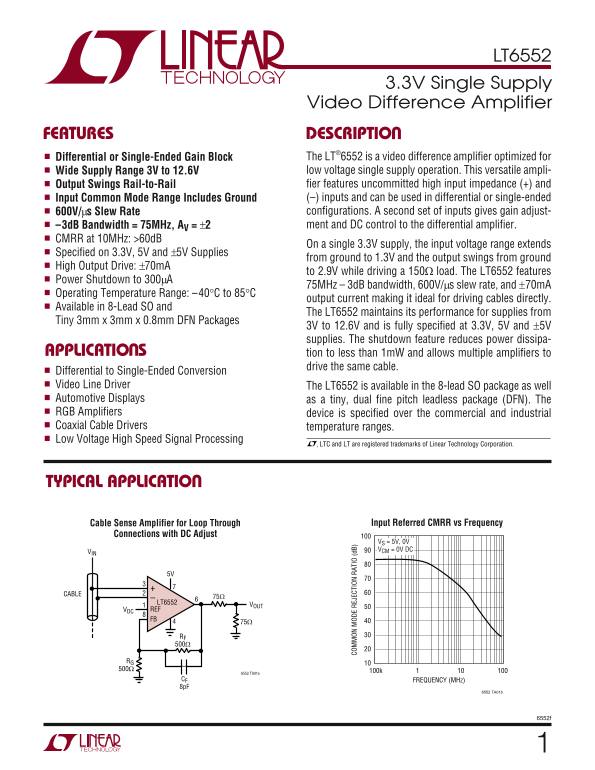
TYPICAL APPLICATIO

Input Referred CMRR vs Frequency Cable Sense Amplifier for Loop Through

Connections with DC Adjust

VS = 5V, 0V VCM = 0V DC

CABLE

75Ω 6LT6552

VDC REF FB

RF 500Ω

RG 500Ω 100k

6552 TA01a

CF FREQUENCY (MHz) 8p F

6552 TA01b

Page Summary Contents For LINEAR TECHNOLOGY LT6552 User's Manual

Page 1 LT6552 3.3V Single Supply Video Difference Amplifier FEATURES DESCRIPTIO Differential or Single-Ended Gain Block The LT®6552 is a video difference amplifier optimized for Wide Supply Range 3V to 12.6V...
Page 2 LT6552 ABSOLUTE AXI RATI GS (Note 1) Supply Voltage (V+ to V–) 12.6V Specified Temperature Range (Note 5) ....–40°C to 85°C Input Current (Note 2) ±10m A Maximum Junction Temperature 150°C Input Volta...
Page 3 LT6552 3.3V ELECTRICAL CHARACTERISTICS The ● denotes the specifications which apply over the full operating temperature range, otherwise specifications are at TA = 25°C. VS = 3.3V, 0V. Figure 1 shows ...
Page 4 LT6552 5V ELECTRICAL CHARACTERISTICS The ● denotes the specifications which apply over the full operating temperature range, otherwise specifications are at TA = 25°C. VS = 5V, 0V; Figure 1 shows the ...
Page 5 LT6552 5V ELECTRICAL CHARACTERISTICS The ● denotes the specifications which apply over the full operating temperature range, otherwise specifications are at TA = 25°C. VS = 5V, 0V. Figure 1 shows the ...
Page 6 LT6552 ±5V ELECTRICAL CHARACTERISTICS The ● denotes the specifications which apply over the full operating temperature range, otherwise specifications are at TA = 25°C. VS = ±5V. Figure 2 shows the DC...
Page 7 SH UT DO PI CU RR EN (µ A) OU TP UT IG SA TU RA TI ON OL TA GE (V SU PP LY UR RE NT (m A) LT6552 TYPICAL PERFOR A CE CHARACTERISTICS Input Bias Current vs Common Supply Current vs Supply Voltage Input...
Page 8 PHASE (DEG) CH AN GE IN IN PU OF FS ET OL TA GE (µ V) GA IN AN DW ID TH CL OS ED -L OO VO LT AG GA IN (d B) LT6552 PR OD UC (M Hz TYPICAL PERFOR A CE CHARACTERISTICS Input Noise Voltage Density vs Inp...
Page 9 CO ON OD RE JE CT IO RA TI (d B) TP UT IM PE DA NC (Ω LT6552 TYPICAL PERFOR A CE CHARACTERISTICS RL = 150Ω TA = 25°C DI ST OR TI ON (d B) VOUT = –3V TO 3V VS = ±5V Output Impedance vs Frequency Slew R...
Page 10 V/ DI 0m V/ DI LT6552 TYPICAL PERFOR A CE CHARACTERISTICS Large Signal Response, Large Signal Response, Small Signal Response, VS = 5V, 0V VS = ±5V VS = 5V, 0V 1V /D IV AV = 2 AV = 2 AV = 1 50ns/DIV50...
Page 11 LT6552 APPLICATIO S I FOR ATIO The LT6552 is a video difference amplifier with two pairs applied to Pin 8 and the LT6552’s transient response is of high impedance inputs. The primary purpose of the op...
Page 12 LT6552 APPLICATIO S I FOR ATIO Amplifier Characteristics The current generated through R1 or R2, divided by the capacitor CM, determines the slew rate. Note that this Figure 5 shows a simplified schem...
Page 13 LT6552 V/ DI APPLICATIO S I FOR ATIO Layout and Passive Components Operating with Low Closed-Loop Gains With a bandwidth of 75MHz and a slew rate of 600V/µs, the The LT6552 has been optimized for clos...
Page 14 LT6552 APPLICATIO S I FOR ATIO SHDN Pin The LT6552 includes a shutdown feature that disables the is 0.25µA (V– ≤ VOUT ≤ V+). In normal operation the SHDN part, reducing quiescent current and making th...
Page 15 LT6552 PACKAGE DESCRIPTIO S8 Package 8-Lead Plastic Small Outline (Narrow .150 Inch) (Reference LTC DWG # 05-08-1610) NOTE 3 .050 BSC MIN .150 – .157 NOTE 3 .030 ±.005 TYP RECOMMENDED SOLDER PAD LAYOU...
Page 16 LT6552 TYPICAL APPLICATIO YPBPR to RGB Video Converter REF 75Ω REF LT6552 LT6552 PR REF 75Ω LT6552 REF 75Ω LT6552 R = Y + 1.4 • PR BW (± 0.5d B) > 25MHz G = Y – 0.34 • PB – 0.71 • PR BW (–3d B) &gt...