# A B C D E F G H I J K L M N O P Q R S T U V W X Y Z

LINEAR TECHNOLOGY LTC1879 User's Manual

Summary

The LTC1879 is a high-efficiency synchronous buck regulator designed for sophisticated power management in portable electronics. This detailed manual provides engineers with comprehensive specifications and application guidance for the device, which delivers up to 95% efficiency while maintaining an ultra-low quiescent current (15mA). Ideal for designers of cellular phones, wireless modems, and battery-powered systems requiring stable voltage regulation across a wide input range (2.65V–10V). Learn about its constant frequency operation, advanced modes like Burst Mode, and robust protection features to ensure optimal battery life and performance in demanding applications.
📄 Preview PAGE OF 20

Page 1 Text Content

LTC1879

1.2A Synchronous

Step-Down Regulator with 15µA Quiescent Current

FEATURES DESCRIPTIO High Efficiency: Up to 95% The LTC®1879 is a high efficiency monolithic synchro- Low Quiescent Current: Only 15µA with No Load nous buck regulator using a constant frequency, current 550k Hz Constant Frequency Operation mode architecture. Operating supply current is only 15µA

2.65V to 10V Input Voltage Range with no load and drops to <1µA in shutdown. The input VOUT from 0.8V to VIN, IOUT to 1.2A supply voltage range of 2.65V to 10V makes the LTC1879 True PLL Frequency Locking from 350k Hz to 750k Hz ideally suited for both single and dual Li-Ion battery-pow- Power Good Output Voltage Monitor ered applications. 100% duty cycle provides low dropout Low Dropout Operation: 100% Duty Cycle operation, extending battery life in portable systems.

Burst Mode® or Pulse Skipping Operation

The switching frequency is internally set to 550k Hz, allow-

Current Mode Operation for Excellent Line and Load

ing the use of small surface mount inductors and capaci-

Transient Response

tors. For noise sensitive applications, the LTC1879 can be

Shutdown Mode Draws <1µA Supply Current

externally synchronized from 350k Hz to 750k Hz. Burst

±2% Output Voltage Accuracy

Mode operation is inhibited during synchronization or

Overcurrent and Overtemperature Protected

when the SYNC/MODE pin is pulled low.

Available in 16-Lead SSOP Package EF FI CI EN CY

The internal synchronous rectifier switch increases effi- ciency and eliminates the need for an external Schottky

APPLICATIO S diode. Low output voltages are easily supported with a

0.8V feedback reference voltage. The LTC1879 is available

Cellular Telephones

in a 16-lead SSOP package.

Portable Computers

, LTC and LT are registered trademarks of Linear Technology Corporation.

Wireless Modems

Burst Mode is a registered trademark of Linear Technology Corporation.

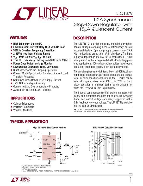
TYPICAL APPLICATIO

High Efficiency Step-Down Converter Efficiency vs Output Load Current VIN

2.65V TO 10V

CIN VIN = 3.6V

10µF SVIN

RUN/SS PVIN

VIN = 7.2V

SYNC/MODE SWP 6.2µH

VOUT* VIN = 10V

LTC1879

PGOOD SWN

150k COUT

ITH PGND 47µF

Burst Mode OPERATION

VFB VOUT = 3.1V SGND 80.6k L = 6.2µH

1879 TA01a OUPUT CURRENT (m A)

CIN: TAIYO YUDEN CERAMIC LMK325BJ106MN 1879 TA01b

COUT: TDK CERAMIC C4532X5ROJ476M L1: TOKO A921CY6R2M *VOUT CONNECTED TO VIN (MINUS SWITCH AND L1 VOLTAGE DROP) FOR 2.65V < VIN < 3.1V

Page Summary Contents For LINEAR TECHNOLOGY LTC1879 User's Manual

Page 1 LTC1879 1.2A Synchronous Step-Down Regulator with 15µA Quiescent Current FEATURES DESCRIPTIO High Efficiency: Up to 95% The LTC®1879 is a high efficiency monolithic synchro- Low Quiescent Current: Onl...
Page 2 LTC1879 ABSOLUTE MAXIMUM RATINGS PACKAGE/ORDER INFORMATION (Note 1) ORDER PART Input Supply Voltage –0.3V to 11V TOP VIEW NUMBER ITH, PLL_LPF Voltages –0.3V to 2.7V SGND PLL_LPF RUN/SS, VFB Voltages –...
Page 3 SU PP LY UR RE NT (µ A) S( ON ) ( LTC1879 ELECTRICAL CHARACTERISTICS The ● denotes specifications which apply over the full operating temperature range, otherwise specifications are TA = 25°C. VIN = 5...
Page 4 RE FE RE NC VO LT AG (m V) SW IT CH EA KA GE (µ A) LTC1879 TYPICAL PERFOR A CE CHARACTERISTICS EF FI CI EN CY Switch Leakage vs Temperature Switch Leakage vs Input Voltage Output Voltage vs Load Curre...
Page 5 LTC1879 TYPICAL PERFOR A CE CHARACTERISTICS Load Step Load Step (Burst Mode Operation) (Pulse Skipping Mode) Soft-Start with Shorted Output IL IL 1A/DIV 1A/DIV IVIN 500m A/DIV RUN/SS VOUT VOUT 1V/DIV ...
Page 6 LTC1879 PI FU CTIO S SGND (Pin 1): Signal Ground Pin. PVIN1, PVIN2 (Pins 8, 9): Power Supply Pins for the Internal Drivers and Switches. These pins should always RUN/SS (Pin 2): Combination of Soft-St...
Page 7 LTC1879 BLOCK DIAGRA BU RS DE FE AT “0 ON LY HE IS ON ST AN “1 PL L_ LP SL OP SV IN SY NC /M OD VC CO AN 0. 8V OS OS FR EQ SH IF EN –+ SL EE PV IN 0. 8V OM EA BU RS –+ SL EE SV IN SW IT CH IN OS FE LO...
Page 8 LTC1879 OPERATIO (Refer to Block Diagram) Main Control Loop the ITH voltage drops below approximately 0.45V, the BURST comparator trips, turning off both power MOSFETs. The LTC1879 uses a constant fre...
Page 9 LTC1879 OPERATIO (Refer to Block Diagram) Power Good Indicator Low Dropout Operation The power good function monitors the output voltage in all When the input supply voltage decreases toward the modes...
Page 10 LTC1879 OPERATIO Slope Compensation and Inductor Peak Current VIN = 5V Slope compensation is required in order to prevent sub- harmonic oscillation at high duty cycles. It is accom- plished by interna...
Page 11 LTC1879 APPLICATIO S I FOR ATIO CIN and COUT Selection The selection of COUT is driven by the required effective series resistance (ESR). Typically, once the ESR require- In continuous mode, the sourc...
Page 12 LTC1879 OS FR EQ UE CN (k Hz APPLICATIO S I FOR ATIO 0.8V ≤ VOUT ≤ 10V RLP R1 CLP PLL_LPF LTC1879 R2 SYNC/ MODE DIGITAL PHASE/ SGND VCO FREQUENCY 1879 F04 DETECTOR Figure 4. Setting the LTC1879 Output...
Page 13 LTC1879 PO ER OS (W APPLICATIO S I FOR ATIO Where ρ1, ρ2, etc. are the individual losses as a percent- 2. I2R losses are calculated from the resistances of the age of input power. internal switches RS...
Page 14 LTC1879 APPLICATIO S I FOR ATIO where TA is the ambient temperature. Because the power Checking Transient Response transistor RDS(ON) is a function of temperature, it is The regulator loop response ca...
Page 15 LTC1879 APPLICATIO S I FOR ATIO PC Board Layout Checklist 3. The high di/dt loop from the top terminal of the input capacitor, through the power MOSFETs and back to the As with all high frequency swit...
Page 16 LTC1879 APPLICATIO S I FOR ATIO Design Example An 15µH inductor works well for this application. For good efficiency choose a 1.5A inductor with less than 0.125Ω As a design example, assume the LTC187...
Page 17 LTC1879 APPLICATIO S I FOR ATIO RSVIN 10Ω CSVIN 0.1µF RPG 100k SVIN SYNC/MODE PGOOD PVIN 2.65V TO 8.4V RSS PVIN 1M GND RUN/SS CSS PGND EF FI CI EN CY COUT LTC1879 47µF SWP L1 15µH PLL_LPF 2.5V SWN 0.7...
Page 18 LTC1879 TYPICAL APPLICATIO Dual Li-Ion to 1.8V/1A Regulator Using All Ceramic Capacitors RSVIN 10Ω CSVIN 0.1µF RPG 100k SVIN SYNC/MODE FI CI EN CY PGOOD PVIN 3V TO 8.4V RSS PVIN 1M GND RUN/SS CSS PGND...
Page 19 LTC1879 PACKAGE DESCRIPTION GN Package 16-Lead Plastic SSOP (Narrow .150 Inch) (Reference LTC DWG # 05-08-1641) .009 (0.229) REF .254 MIN .150 – .165 .0015 .0250 TYP.0165 ± RECOMMENDED SOLDER PAD LAYO...
Page 20 LTC1879 TYPICAL APPLICATIO 5-Cell Ni MH to 3.3V/0.25A ZETA Regulator Using All Ceramic Capacitors RSVIN 10Ω CSVIN 0.1µF 100k SVIN SYNC/MODE PGOOD PVIN CIN2 2.8V TO 7.5V RSS CIN1 PVIN 10µF RUN/SS CSS P...

Manual Details

Brand Linear
Pages 20
File Size 256.26 KB
Published May 30, 2026
70 views

Enter the captcha to get the download link:

captcha

Frequently Asked Questions

What is the input voltage range for the LTC1879?

The IC operates with an input voltage range of 2.65V to 10V.

How low can the device draw power when idle?

It drops to less than 1mA in shutdown mode.

What cycle frequency is best for battery applications?

The internal synchronous rectifier switch increases efficiency, eliminating the need for external Schottky diodes.

Can this converter support multiple voltage outputs?

Yes, it supports a 'Power Good Output Voltage Monitor' and can monitor voltage drops while operating in bursts.