# A B C D E F G H I J K L M N O P Q R S T U V W X Y Z

LINEAR TECHNOLOGY LTC3731 User's Manual

Summary

The LTC3731 is a powerful, high-efficiency synchronous three-phase buck switching regulator controller designed for demanding DC/DC power solutions. This resource details critical features such as phase-lockable frequency generation up to 600kHz per phase and advanced protection against overcurrent and undervoltage. It empowers electrical engineers and designers of high-output current systems, including servers and desktop computer infrastructure, requiring precise power delivery and optimal thermal management.
📄 Preview PAGE OF 32

Page 1 Text Content

LTC3731

3-Phase, 600k Hz,

Synchronous Buck Switching

Regulator Controller FEATURES DESCRIPTIO 3-Phase Current Mode Controller with Onboard The LTC®3731 is a Poly Phase® synchronous step-down MOSFET Drivers switching regulator controller that drives all N-channel ex-

±5% Output Current Matching Optimizes Thermal ternal power MOSFET stages in a phase-lockable fixed fre- Performance and Size of Inductors and MOSFETs quency architecture. The 3-phase controller drives its Differential Amplifier Accurately Senses VOUT output stages with 120° phase separation at frequencies of ±1% VREF Accuracy Over Temperature up to 600k Hz per phase to minimize the RMS current losses Reduced Power Supply Induced Noise in both the input and output filter capacitors. The 3-phase ±10% Power Good Output Indicator technique effectively triples the fundamental frequency, 250k Hz to 600k Hz Per Phase, PLL, Fixed Frequency improving transient response while operating each control- ler at an optimal frequency for efficiency and ease of ther-

PWM, Stage Shedding TM or Burst Mode® Operation

mal design. Light load efficiency is optimized by using a

OPTI-LOOP® Compensation Minimizes COUT

choice of output Stage Shedding or Burst Mode operation.

Adjustable Soft-Start Current Ramping Short-Circuit Shutdown Timer with Defeat Option A differential amplifier provides true remote sensing of both Overvoltage Soft Latch the high and low side of the output voltage at the point of Adjustable Undervoltage Lockout Threshold load. The precision reference supports output voltages from Selectable Phase Output for Up to 12-Phase Operation 0.6V to 6V. Available in 5mm × 5mm QFN and 36-Pin Narrow

Soft-start and a defeatable, timed short-circuit shutdown

(0.209") SSOP Packages

protect the MOSFETs and the load. Current foldback provides protection for the external MOSFETs under

APPLICATIO

short-circuit or overload conditions.

Desktop Computers and Servers , LTC and LT are registered trademarks of Linear Technology Corporation. Burst Mode,

OPTI-LOOP and Poly Phase are registered trademarks of Linear Technology Corporation.

High Performance Notebook Computers

Stage Shedding is a trademark of Linear Technology Corporation. All other trademarks are the property of their respective owners. Protected by U.S. Patents, including 5481178,

High Output Current DC/DC Power Supplies

TYPICAL APPLICATIO

VCC 5V TO 28V

TG1VCC

4.5V TO 7V 0.003Ω0.8µH

LTC3731 22µF

10µF SW1

BOOST1

BOOST2 BOOST3

0.1µF SENSE1+ SENSE1–

SW3 SW2 SW1 VIN

POWER GOOD INDICATOR PGOOD 0.003Ω0.8µH VOUT

OPTIONAL SYNC IN PLLIN SW2 1.35V

PLLFLTR BG2 36k PGND

VIN UVADJ

SENSE2+

680p F SENSE2–

ITH TG3

5k RUN/SS

0.01µF SGND BG3 EAIN 100p F

DIFFOUT SENSE3+

SENSE3–IN– COUT

IN+ 470µF

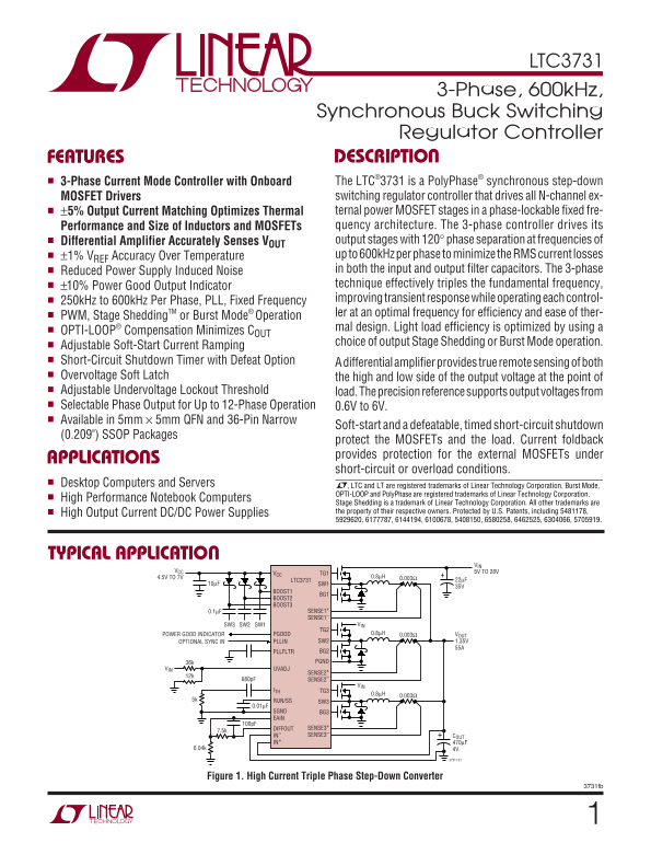
Figure 1. High Current Triple Phase Step-Down Converter

3731fb

Page Summary Contents For LINEAR TECHNOLOGY LTC3731 User's Manual

Page 1 LTC3731 3-Phase, 600k Hz, Synchronous Buck Switching Regulator Controller FEATURES DESCRIPTIO 3-Phase Current Mode Controller with Onboard The LTC®3731 is a Poly Phase® synchronous step-down MOSFET Dr...
Page 2 LTC3731 ABSOLUTE AXI U RATI GS (Note 1) Topside Driver Voltages (BOOSTN) 38V to –0.3V ITH Voltage 2.4V to –0.3V Switch Voltage (SWN)................................... 32V to –5V Operating Ambient Tem...
Page 3 LTC3731 ELECTRICAL CHARACTERISTICS The ● denotes the specifications which apply over the full operating temperature range, otherwise specifications are at TA = 25°C. VCC = VRUN/SS = 5V unless otherwis...
Page 4 LTC3731 ELECTRICAL CHARACTERISTICS The ● denotes the specifications which apply over the full operating temperature range, otherwise specifications are at TA = 25°C. VCC = VRUN/SS = 5V unless otherwis...
Page 5 LTC3731 PI FU CTIO S BG1 to BG3: High Current Gate Drives for Bottom N-Channel PLLIN: Synchronization Input to Phase Detector. This pin is MOSFETs. Voltage swing at these pins is from ground to VCC. i...
Page 6 FR EQ UE NC (k Hz RE FE RE NC VO LT AG (m V) EF FI CI EN CY LTC3731 TYPICAL PERFOR A CE CHARACTERISTICS Efficiency vs IOUT (Figure 14) Efficiency vs VIN (Figure 14) Efficiency vs Frequency (Figure 14)...
Page 7 PE AK EN SE OL TA GE (m V) AX IM UM (m V) RU N/ SS IN OL TA GE (V EN SE LTC3731 TYPICAL PERFOR A CE CHARACTERISTICS Short-Circuit Arming and Latchoff RUN/SS Pull-Up Current vs vs Temperature Supply Cu...
Page 8 LTC3731 TYPICAL PERFOR A CE CHARACTERISTICS Differential Amplifier Gain-Phase GA IN (d B) PHASE (DEG) –9 –135 0.01 0.1 FREQUENCY (MHz) Shed Mode at 1 Amp, Light Load Burst Mode at 1 Amp, Light Load Cu...
Page 9 LTC3731 FU CTIO AL DIAGRA PLLIN FIN PHASE DET RLP PLLFLTR CLP CLKOUT CLK1 OSCILLATOR CLK2 PHASMD** CLK3 DUPLICATE FOR SECOND AND THIRD VCC VIN PGOOD** 0.66V CONTROLLER CHANNELS BOOST DELAY DROP OUT 0....
Page 10 LTC3731 OPERATIO (Refer to Functional Diagram) Main Control Loop Low Current Operation The IC uses a constant frequency, current mode step- The FCB pin is a logic input to select between three modes d...
Page 11 LTC3731 OPERATIO (Refer to Functional Diagram) C) Continuous Current Operation errors caused by board-to-board interconnects, particu- larly helpful in VRM designs. Tying the FCB pin to ground will fo...
Page 12 LTC3731 OPERATIO (Refer to Functional Diagram) the RUN/SS pin voltage is recycled. This built-in latchoff Input Undervoltage Reset can be overridden by providing >5µA at a compliance of The RUN/SS ...
Page 13 LTC3731 APPLICATIO S I FOR ATIO current and low current operation must also be consid- 1-PHASE 0.9 2-PHASE ered. The Poly Phase approach reduces both input and 3-PHASE 4-PHASE output ripple currents w...
Page 14 LTC3731 APPLICATIO S I FOR ATIO Power MOSFET and D1, D2, D3 Selection stage and then plotting the gate voltage versus time. The initial slope is the effect of the gate-to-source and the gate- At least...
Page 15 LTC3731 APPLICATIO S I FOR ATIO where N is the number of output stages, δ is the tempera- can be found in Application Note 77. Figure 6 shows the ture dependency of RDS(ON), RDR is the effective top d...
Page 16 LTC3731 APPLICATIO S I FOR ATIO size or height requirements in the design. Always consult where f = operating frequency of each stage, N is the the capacitor manufacturer if there is any question. num...
Page 17 LTC3731 APPLICATIO S I FOR ATIO special polymer capacitors available in case heights Topside MOSFET Driver Supply (CB, DB) ranging from 2mm to 4mm. Other capacitor types in- External bootstrap capacit...
Page 18 LTC3731 APPLICATIO S I FOR ATIO Soft-Start/Run Function The RUN/SS pin has an internal 6V zener clamp (see the Functional Diagram). The RUN/SS pin provides three functions: 1) ON/OFF, 2) soft-start an...
Page 19 LTC3731 APPLICATIO S I FOR ATIO The value of the soft-start capacitor CSS may need to be Undervoltage Reset scaled with output current, output capacitance and load In the event that the input power so...
Page 20 LTC3731 APPLICATIO S I FOR ATIO PHASE 10k If the duty cycle falls below what can be accommodated by DETECTOR/ OSCILLATOR the minimum on-time, the IC will begin to skip every other EXTERNAL cycle, resu...
Page 21 LTC3731 APPLICATIO S I FOR ATIO time, VOUT can be monitored for excessive overshoot or A second, more severe transient is caused by switching in ringing, which would indicate a stability problem. The ...
Page 22 LTC3731 APPLICATIO S I FOR ATIO Use a commonly available 0.003Ω sense resistor. VCC Next verify the minimum on-time is not violated. The 5V minimum on-time occurs at maximum VCC: ns ON LTC3731 IN MAX ...
Page 23 LTC3731 APPLICATIO S I FOR ATIO which is less than one third of the normal, full load PC Board Layout Checklist conditions. Incidentally, since the load no longer dissi- When laying out the printed ci...
Page 24 LTC3731 APPLICATIO S I FOR ATIO 1) Are the signal and power ground paths isolated? Keep the 4) Do the (+) plates of CPWR connect to the drains of the SGND at one end of a printed circuit path thus pre...
Page 25 LTC3731 APPLICATIO S I FOR ATIO Simplified Visual Explanation of How a 3-Phase levels with the addition of more phases. A higher effective Controller Reduces Both Input and Output RMS duty factor resu...
Page 26 LTC3731 APPLICATIO S I FOR ATIO The ripple frequency is also increased by three, further The main MOSFET is on for the duty factor VOUT/VIN and reducing the required output capacitance when VCC < 3...
Page 27 LTC3731 PACKAGE DESCRIPTIO This totals 1W at VIN = 8V, 2.25W at VIN = 12V and 6.25W The total output power is (1.3V)(45A) = 58.5W and the at VIN = 20V. total input power is approximately 60W so the % ...
Page 28 LTC3731 TYPICAL APPLICATIO Figure 14. 3-Phase 65A Power Supply 1µF VCC OPTIONAL FILTER FOR 10Ω SYNCHRONIZATION 1000p F PGOOD VCC VCC CLK NC SYNC IN VCC 0.01µF PLLIN PGOOD 10k 300k Hz 5V TO 7V PLLFLTR ...
Page 29 LTC3731 TYPICAL APPLICATIO Figure 15. 2.5V/100A Power Supply VCC V5 PGOOD BOOST1 BOOST3 VCC VCC CLKOUT CLK1 BOOST2 VCC Cer. 10V CLKOUT PLLIN PGOOD PLLFLTR BOOST1 1Ω VIN FCB TG1 M1 L1 VOUTS IN+ SW1 220...
Page 30 LTC3731 PACKAGE DESCRIPTIO G Package 36-Lead Plastic SSOP (5.3mm) (Reference LTC DWG # 05-08-1640) 0.42 ±0.03 0.65 BSC RECOMMENDED SOLDER PAD LAYOUT BSC 0.05 NOTE: (.002) 1. CONTROLLING DIMENSION: MIL...
Page 31 LTC3731 PACKAGE DESCRIPTIO UH Package 32-Lead Plastic QFN (5mm × 5mm) (Reference LTC DWG # 05-08-1693) 3.45 ±0.05 (4 SIDES) PACKAGE OUTLINE 0.25 ± 0.05 0.50 BSC RECOMMENDED SOLDER PAD LAYOUT BOTTOM VI...
Page 32 LTC3731 RELATED PARTS PART NUMBER DESCRIPTION COMMENTS LTC1628/LTC3728 2-Phase, Dual Output Synchronous Step-Down Reduces CIN and COUT, Power Good Output Signal, Synchronizable, DC/DC Controllers 3.5V...

Manual Details

Brand Linear
Pages 32
File Size 373.10 KB
Published June 01, 2026
89 views

Enter the captcha to get the download link:

captcha

Frequently Asked Questions

What phase separation does the LTC3731 offer?

It offers 120° phase separation at frequencies up to 600kHz per phase.

How can I enhance the transient response and efficiency for this regulator?

Use the Reduced Power Supply Induced Noise technique, which triples the fundamental frequency, or use adjustable Soft-Start/Burst Mode operation.

What protection features are available on the controller?

It includes Short-Circuit Shutdown Timer with defeat option, Overvoltage Soft Latch, and Adjustable Undervoltage Lockout Thresholds.

Does this regulator support multiple output phases?

Yes, it supports selectable phase output for up to 12-Phase Operation.