# A B C D E F G H I J K L M N O P Q R S T U V W X Y Z

LINEAR TECHNOLOGY LTC3219 User's Manual

Summary

The LTC3219 is a highly integrated, multi-mode LED driver designed for complex display applications. This chip provides power to up to nine independent LED current sources, offering exceptional efficiency via its charge pump architecture (operating in various modes) and advanced thermal/short-circuit protection. The device allows designers granular control over brightness, dimming, and On/Off status for every channel using a simple I²C serial interface. Ideal for electronics professionals designing portable devices, video phones, or custom lighting solutions requiring high performance and precise LED management.
📄 Preview PAGE OF 20

Page 1 Text Content

LTC3219

250m A Universal

Nine Channel LED Driver

FEATURES DESCRIPTION ■ Multimode Charge Pump Provides Up to 91%

The LTC®3219 is a highly integrated multidisplay LED

Effi ciency driver. The device contains a high effi ciency, low noise ■ Slew Limited Switching Reduces Conducted and

charge pump to provide power to nine universal LED

Radiated Noise (EMI) current sources. The LTC3219 requires only fi ve small ■ Up to 250m A Total Output Current

ceramic capacitors to form a complete LED power supply

■ Nine 28m A Universal Current Sources with 64-Step

and current controller.

Linear Brightness Control

The maximum display currents are set by an internal pre-

■ Independent On/Off, Brightness Level, Blinking and

cision current reference. Independent dimming, On/Off,

Gradation Control for Each Current Source Using

blinking and gradation control for all current sources is

2-Wire I2CTM Interface

achieved via the I2C serial interface. 6-bit linear DACs are

■ Internal Current Reference

available for adjusting brightness levels for each universal

■ Confi gurable ENU Pin for Asynchronous LED On/Off

LED current source.

Control ■ Low Noise Charge Pump Operates in 1x, 1.5x or 2x The LTC3219 charge pump optimizes effi ciency based on

Mode for Optimal Effi ciency* the voltage across the LED current sources. The device

■ Automatic or Forced Mode Switching powers up in 1x mode and will automatically switch to ■ Internal Soft-Start Limits Inrush Current boost mode whenever any enabled LED current source ■ Short-Circuit/Thermal Protection begins to enter dropout. The fi rst dropout switches the ■ 3mm × 3mm 20-Lead QFN Plastic Package IC into 1.5x mode and a subsequent dropout switches

the LTC3219 into 2x mode. The part resets to 1x mode APPLICATIONS whenever a data register is updated via the I2C port. , LT, LTC and LTM are registered trademarks of Linear Technology Corporation.

■ Video Phones with QVGA+ Displays

All other trademarks are the property of their respective owners. *Protected by U.S. Patents, including 6411531.

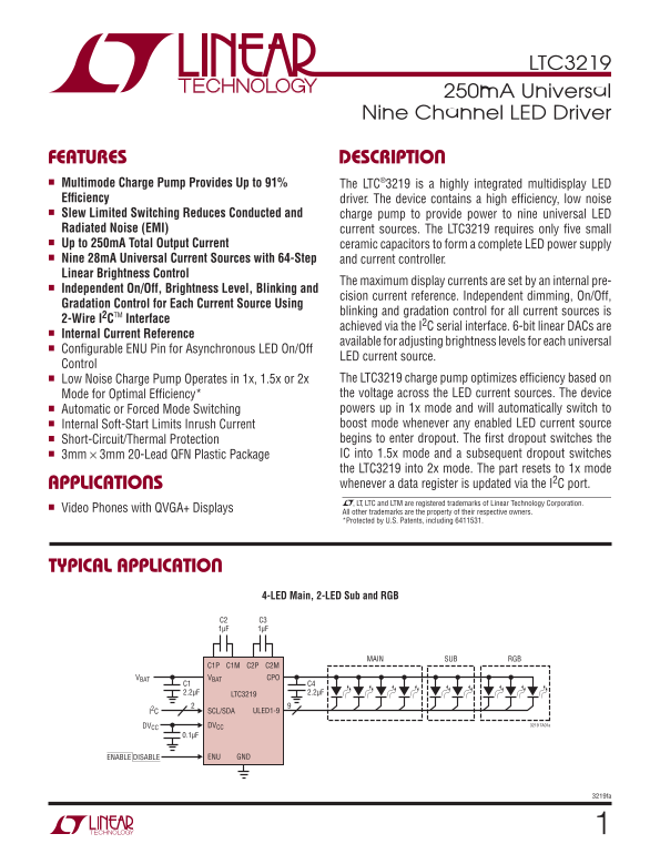
TYPICAL APPLICATION

4-LED Main, 2-LED Sub and RGB

MAIN SUB RGB

C1P C1M C2P C2M VBATVBAT CPO C1 C4 2.2μF LTC3219 2.2μF

I2C SCL/SDA ULED1-9

DVCC DVCC 3219 TA01a

ENABLE DISABLE ENU GND

3219fa

Page Summary Contents For LINEAR TECHNOLOGY LTC3219 User's Manual

Page 1 LTC3219 250m A Universal Nine Channel LED Driver FEATURES DESCRIPTION ■ Multimode Charge Pump Provides Up to 91% The LTC®3219 is a highly integrated multidisplay LED Effi ciency driver. The device con...
Page 2 LTC3219 ABSOLUTE MAXIMUM RATINGS PIN CONFIGURATION (Notes 1, 4) VBAT, DVCC, CPO ........................................... –0.3V to 6V TOP VIEW ULED1-ULED9 ..............................................
Page 3 LTC3219 ELECTRICAL CHARACTERISTICS The ● denotes the specifi cations which apply over the full operating temperature range, otherwise specifi cations are at TA = 25°C. VBAT = 3.6V, DVCC = 3V, ENU = Hi...
Page 4 -L IS TA IT IS TA LTC3219 TYPICAL PERFORMANCE CHARACTERISTICS TA = 25°C unless otherwise noted. Mode Switch Dropout Times 1.5x Mode CPO Ripple 2x Mode CPO Ripple VBAT = 3.6V VBAT = 3.6V VBAT = 3.6V IC...
Page 5 LTC3219 TYPICAL PERFORMANCE CHARACTERISTICS TA = 25°C unless otherwise noted. VBAT Shutdown Current 1x Mode No Load VBAT Current vs vs VBAT Voltage VBAT Voltage 7.5 TA = –40°C TA = 25°C TA = 85°C IN L...
Page 6 LTC3219 PIN FUNCTIONS CPO (Pin 1): Output of the Charge Pump Used to Power ENU (Pin 10): Input. Used to enable or disable the pre- all LEDs. A 2.2μF X5R or X7R ceramic capacitor should selected ULED o...
Page 7 LTC3219 BLOCK DIAGRAM 850k Hz OSCILLATOR CHARGE PUMP 9 UNIVERSAL CURRENT SOURCES AND DACS U7 ENU CONTROL LOGIC U9 MASTER/SLAVE REG SHIFT REGISTER 3219 BD 3219fa
Page 8 LTC3219 OPERATION Power Management Charge Pump Strength The LTC3219 uses a switched capacitor charge pump to When the LTC3219 operates in either 1.5x mode or 2x mode, boost CPO to as much as 2 times t...
Page 9 LTC3219 OPERATION Mode Switching Blinking The LTC3219 will automatically switch from 1x mode to 1.5x Each universal output (ULED1 to ULED9) can be set to mode and subsequently to 2x mode whenever a dr...
Page 10 LTC3219 OPERATION To use the ENU pin, the I2C port must fi rst be confi gured in shutdown. Internal logic ensures that the LTC3219 is to select the desired LED outputs. When ENU is high, the in shutdo...
Page 11 LTC3219 OPERATION I2C Interface The LTC3219 is a receive-only (slave) device. The LTC3219 communicates with a host (master) using Write Word Protocol Used by the LTC3219 the standard I2C 2-wire interf...
Page 12 LTC3219 OPERATION Sub-Address Byte MSB LSB Register Function REG0 COMMAND REG1 ULED1 REG2 ULED2 REG3 ULED3 REG4 ULED4 REG5 ULED5 REG6 ULED6 REG7 ULED7 REG8 ULED8 REG9 ULED9 REG10 ENU REG11 B/G/ENU REG...
Page 13 LTC3219 OPERATION Data Bytes REG1 to REG9, Universal LED 6-bit linear DAC data with blink/gradation. Sub-Address 0001 TO 1001 per Sub-Address Table Above ULED Mode Enable Bits LED Current Data MSB LSB...
Page 14 LTC3219 OPERATION Bus Speed to recognize the address since it is a write only device. This effectively forces the address to be eight bits long The I2C port is designed to be operated at speeds of up ...
Page 15 LTC3219 OPERATION to any Stop that appears on the bus with only one excep- Quick Write tion, independent of the number of Repeat-Start’s that Registers REG1 to REG9 can be written in parallel by set- ...
Page 16 LTC3219 APPLICATIONS INFORMATION LTC3219 GND 3219 F04 Figure 4. 10n H Inductor Used for Input Noise Reduction (Approximately 1cm of Board Trace) Flying Capacitor Selection Table 1 shows a list of cera...
Page 17 LTC3219 APPLICATIONS INFORMATION Power Effi ciency In 1.5x boost mode, the effi ciency is similar to that of a linear regulator with an effective input voltage of 1.5 times To calculate the power effi...
Page 18 LTC3219 TYPICAL APPLICATIONS Three RGB LED Groups RGB1 RGB2 RGB3 C1P C1M C2P C2M VBATVBAT CPO C1 C4 2.2μF LTC3219 2.2μF I2C SCL/SDA ULED1-9 3219 TA03 DVCCDVCC C5 0.1μF ENU GND 5-LED Main, 4 General Pu...
Page 19 LTC3219 PACKAGE DESCRIPTION UD Package 20-Lead Plastic QFN (3mm × 3mm) (Reference LTC DWG # 05-08-1720 Rev A) 3.50 0.05 (4 SIDES) 1.65 0.05 PACKAGE OUTLINE 0.20 0.05 0.40 BSC RECOMMENDED SOLDER PAD PI...
Page 20 LTC3219 TYPICAL APPLICATION 3-LED Main, 1-LED Sub and 5-LED Camera C2 C3 1μF 1μF MAIN SUB CAM VBATVBAT CPO C1 C4 2.2μF LTC3219 2.2μF I2C SCL/SDA ULED1-3 3219 TA02 DVCC DVCC ULED4 ULED5-9 ENABLE DISABL...

Manual Details

Brand Linear
Pages 20
File Size 216.52 KB
Published June 02, 2026
74 views

Enter the captcha to get the download link:

captcha

Frequently Asked Questions

What operating temperature range does the LTC3219 support?

The device operates in a temperature range of -40°C to 85°C.

How is brightness adjusted for individual current sources?

Brightness control can be achieved via the I²C serial interface using internal 6-bit linear DACs for each source.

What does the LTC3219 automatically switch to during power fluctuations?

It optimizes efficiency by switching from 1x mode to 1.5x mode upon the first dropout, and then to 2x mode upon a subsequent dropout.

Is external soldering required for proper use?

Yes, the Exposed Pad (PIN 21) labeled 'IS' must be soldered to the PCB for grounding.