# A B C D E F G H I J K L M N O P Q R S T U V W X Y Z

LINEAR TECHNOLOGY LTC3448 User's Manual

Summary

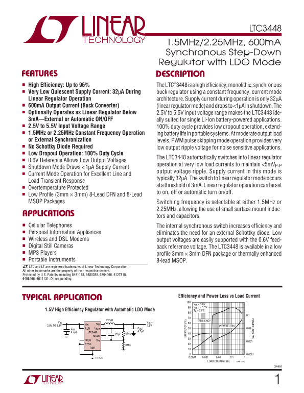
The LTC3448 is a high-efficiency, synchronous step-down regulator perfect for advanced portable electronics applications. This component features automatic low-dropout linear mode (LDO), ultra-low quiescent current (<1µA), and selectable switching frequencies (1.5MHz or 2.25MHz). It maintains stable power regulation across a 2.5V to 5.5V input range, eliminating the need for external Schottky diodes. Ideal for battery-powered devices such as cellular phones, MP3 players, and digital cameras that require maximum efficiency and minimal quiescent current draw.
📄 Preview PAGE OF 20

Page 1 Text Content

LTC3448

1.5MHz/2.25MHz, 600m A

POW ER LOSS (W

Synchronous Step-Down Regulator with LDO Mode

FEATURES DESCRIPTIO High Efficiency: Up to 96% The LTC®3448 is a high efficiency, monolithic, synchronous Very Low Quiescent Supply Current: 32µA During buck regulator using a constant frequency, current mode Linear Regulator Operation architecture. Supply current during operation is only 32µA 600m A Output Current (Buck Converter) (linear regulator mode) and drops to <1µA in shutdown. The Optionally Operates as Linear Regulator Below 2.5V to 5.5V input voltage range makes the LTC3448 ide- 3m A—External or Automatic ON/OFF ally suited for single Li-Ion battery-powered applications. 2.5V to 5.5V Input Voltage Range 100% duty cycle provides low dropout operation, extend- 1.5MHz or 2.25MHz Constant Frequency Operation ing battery life in portable systems. At moderate output load or External Synchronization levels, PWM pulse skipping mode operation provides very No Schottky Diode Required low output ripple voltage for noise sensitive applications. Low Dropout Operation: 100% Duty Cycle

The LTC3448 automatically switches into linear regulator

0.6V Reference Allows Low Output Voltages

operation at very low load currents to maintain <5m VP-P

Shutdown Mode Draws < 1µA Supply Current

output voltage ripple. Supply current in this mode is

Current Mode Operation for Excellent Line and

typically 32µA. The switch to linear regulator mode occurs

Load Transient Response

EF FI CI EN CY at a threshold of 3m A. Linear regulator operation can be set

Overtemperature Protected

to on, off or automatic turn on/off.

Low Profile (3mm × 3mm) 8-Lead DFN and 8-Lead MSOP Packages Switching frequency is selectable at either 1.5MHz or

2.25MHz, allowing the use of small surface mount induc-

APPLICATIO S

tors and capacitors.

Cellular Telephones The internal synchronous switch increases efficiency and Personal Information Appliances eliminates the need for an external Schottky diode. Low Wireless and DSL Modems output voltages are easily supported with the 0.6V feed- Digital Still Cameras back reference voltage. The LTC3448 is available in a low MP3 Players profile 3mm × 3mm DFN package or thermally enhanced Portable Instruments 8-lead MSOP. , LTC and LT are registered trademarks of Linear Technology Corporation. All other trademarks are the property of their respective owners. Protected by U.S. Patents including 5481178, 6580258, 6304066, 6127815, 6498466, 6611131. Others pending.

Efficiency and Power Loss vs Load Current

TYPICAL APPLICATIO

VIN = 3.6V VOUT = 1.5V

1.5V High Efficiency Regulator with Automatic LDO Mode TA = 25°C

2.2µH EFFICIENCY

VIN VOUT

VIN SW

2.5V TO 5.5V 1.5V POWER LOSS

CIN RUN VOUT COUT 0.01 4.7µF 4.7µF

LTC3448

MODE FREQ VFB

SYNC 316k GND

3448 TA01a 0.0001 0.001 0.01 0.1

LOAD CURRENT (A) 23448 TA01b

Page Summary Contents For LINEAR TECHNOLOGY LTC3448 User's Manual

Page 1 LTC3448 1.5MHz/2.25MHz, 600m A POW ER LOSS (W Synchronous Step-Down Regulator with LDO Mode FEATURES DESCRIPTIO High Efficiency: Up to 96% The LTC®3448 is a high efficiency, monolithic, synchronous Ve...
Page 2 LTC3448 ABSOLUTE AXI U RATI GS (Note 1) Input Supply Voltage –0.3V to 6V VOUT (LDO) Source Current 25m A RUN, SYNC Voltages –0.3V to (VIN + 0.3V) Peak SW Sink and Source Current 1.3A MODE Voltage –0.3...
Page 3 LTC3448 ELECTRICAL CHARACTERISTICS The ● denotes specifications which apply over the full operating temperature range, otherwise specifications are TA = 25°C. VIN = 3.6V unless otherwise specified. SY...
Page 4 FR EQ UE NC (M Hz EF FI CI EN CY EF FI CI EN CY LTC3448 TYPICAL PERFOR A CE CHARACTERISTICS (From Figure1a Except for the Resistive Divider Resistor Values) Efficiency vs Input Voltage Efficiency vs L...
Page 5 SW IT CH EA KA GE (n A) S( ON ) ( LTC3448 TYPICAL PERFOR A CE CHARACTERISTICS (From Figure1a Except for the Resistive Divider Resistor Values) Dynamic Supply Current Dynamic Supply Current RDS(ON) vs ...
Page 6 LTC3448 TYPICAL PERFOR A CE CHARACTERISTICS (From Figure 1a Except for the Resistive Divider Resistor Values) External Mode Control (Constant Load Step 1m A Load) SWITCHER SWITCHER VOUT 20m V/DIV 100m...
Page 7 LTC3448 FU CTIO AL DIAGRA SYNC MODE SLOPE LDO CONTROL COMP LOGIC DRIVE VFB ICOMP VIN SWITCHING RS LATCH LOGIC AND ANTI- BLANKING SHOOT- 0.6V REF CIRCUIT THRU SW5 OVDET 0.6V + ∆OVL SHUTDOWN GND 3448 F0...
Page 8 LTC3448 (m A) DO (O N) (m A) DO (O N) OPERATIO (Refer to Functional Diagram) the VOUT pin and both the main and synchronous switches Some applications may be able to anticipate the transition are turn...
Page 9 LTC3448 AX IM UM UT PU CU RR EN (m A) OPERATIO (Refer to Functional Diagram) (see Typical Performance Characteristics). Therefore, the user should calculate the power dissipation when the LTC3448 is u...
Page 10 LTC3448 APPLICATIO S I FOR ATIO Inductor Core Selection temperature than required. Always consult the manufac- turer if there is any question. Different core materials and shapes will change the size/...
Page 11 LTC3448 APPLICATIO S I FOR ATIO worst, a sudden inrush of current through the long wires loss dominates the efficiency loss at low load currents, can potentially cause a voltage spike at VIN, large en...
Page 12 LTC3448 APPLICATIO S I FOR ATIO top and bottom MOSFET RDS(ON) and the duty cycle where PD is the power dissipated by the regulator and θJA (DC) as follows: is the thermal resistance from the junction ...
Page 13 LTC3448 APPLICATIO S I FOR ATIO with COUT, causing a rapid drop in VOUT. No regulator can 2. Does the VFB pin connect directly to the feedback deliver enough current to prevent this problem if the loa...
Page 14 LTC3448 APPLICATIO S I FOR ATIO and high load currents is important. Output voltage is CIN will require an RMS current rating of at least 0.3A ≅ 1.8V. With this information we can calculate L using IL...
Page 15 LTC3448 TYPICAL APPLICATIO S Single Li-Ion 1.5V/600m A Regulator for Efficiency vs Output Current High Efficiency and Small Footprint VOUT = 1.5V TA = 25°C VIN 2.2µH* 2.7V VIN SW TO 5.5V CIN RUN VOUT ...
Page 16 LTC3448 TYPICAL APPLICATIO S Single Li-Ion 1.2V/600m A Regulator for High Efficiency and Small Footprint Efficiency vs Output Current VIN 2.2µH* VOUT VOUT = 1.2V 2.7V VIN SW 1.2V TA = 25°C TO 5.5V CIN...
Page 17 LTC3448 TYPICAL APPLICATIO S Single Li-Ion 2.5V/600m A Regulator with 1.8MHz External Synchronization and External MODE 2.2µH VOUT VIN SW 2.5V 2.5V TO 5.5V CIN COUT 600m A RUN VOUT CER LTC3448 CERCFF ...
Page 18 LTC3448 PACKAGE DESCRIPTIO DD Package 8-Lead Plastic DFN (3mm × 3mm) (Reference LTC DWG # 05-08-1698) (2 SIDES)2.15 ±0.05 PACKAGE OUTLINE 0.50 BSC 2.38 ±0.05 (2 SIDES) RECOMMENDED SOLDER PAD PITCH AND...
Page 19 LTC3448 PACKAGE DESCRIPTIO MS8E Package 8-Lead Plastic MSOP (Reference LTC DWG # 05-08-1662) BOTTOM VIEW OF EXPOSED PAD OPTION 0.42 ± 0.038 0.65 (.118 ± .004) 0.52 (.0165 ± .0015) (.0256) (NOTE 3) (.0...
Page 20 LTC3448 RELATED PARTS PART NUMBER DESCRIPTION COMMENTS LT1616 500m A (IOUT), 1.4MHz, High Efficiency Step-Down 90% Efficiency, VIN = 3.6V to 25V, VOUT ≥ 1.25V, IQ = 1.9m A, DC/DC Converter ISD = &lt;1...

Manual Details

Brand Linear
Pages 20
File Size 273.60 KB
Published May 30, 2026
85 views

Enter the captcha to get the download link:

captcha

Frequently Asked Questions

What is the supply current when the LTC3448 unit is in shutdown mode?

The supply current draws less than 1µA.

Can this regulator function as a linear regulator, and if so, what are its operating parameters?

Yes, it automatically switches into linear regulator mode when the load drops below 3mA, and can operate between 2.5V to 5.5V.

Are external components required for proper operation?

No external Schottky diode is required due to the internal synchronous switch.

What are the selectable switching frequencies available on the LTC3448?

It can select between 1.5MHz or 2.25MHz constant frequency operation.