# A B C D E F G H I J K L M N O P Q R S T U V W X Y Z

LINEAR TECHNOLOGY LTC1703 User's Manual

Summary

Engineers seeking high-efficiency power solutions will find the LTC1703 dual synchronous switching regulator controller ideal for advanced mobile or processor supply applications. This device features two independent PWM controllers that operate out-of-phase at 550kHz, supporting low voltages (0.9V to 2.0V) and meeting Intel Mobile VID standards with optional DAC functionality. The comprehensive technical documentation details its electrical specifications, fast transient response, and protection modes like FAULT mode, making it a crucial component for power supply designers building highly regulated Voltage Regulator Modules (VRMs).
📄 Preview PAGE OF 36

Page 1 Text Content

LTC1703

Dual 550k Hz Synchronous 2-Phase Switching Regulator Controller with 5-Bit VID

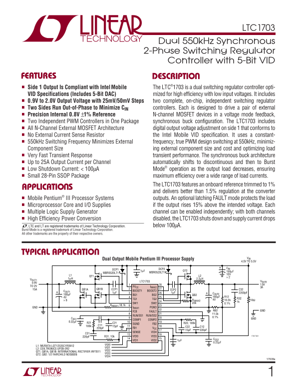
FEATURES DESCRIPTIO Side 1 Output Is Compliant with Intel Mobile The LTC®1703 is a dual switching regulator controller opti- VID Specifications (Includes 5-Bit DAC) mized for high efficiency with low input voltages. It includes 0.9V to 2.0V Output Voltage with 25m V/50m V Steps two complete, on-chip, independent switching regulator

Two Sides Run Out-of-Phase to Minimize CIN controllers. Each is designed to drive a pair of external Precision Internal 0.8V ±1% Reference N-channel MOSFET devices in a voltage mode feedback,

Two Independent PWM Controllers in One Package synchronous buck configuration. The LTC1703 includes

All N-Channel External MOSFET Architecture digital output voltage adjustment on side 1 that conforms to No External Current Sense Resistor the Intel Mobile VID specification. It uses a constant- 550k Hz Switching Frequency Minimizes External frequency, true PWM design switching at 550k Hz, minimiz- Component Size ing external component size and cost and optimizing load Very Fast Transient Response transient performance. The synchronous buck architecture Up to 25A Output Current per Channel automatically shifts to discontinuous and then to Burst Low Shutdown Current: < 100µA Mode® operation as the output load decreases, ensuring

Small 28-Pin SSOP Package maximum efficiency over a wide range of load currents.

The LTC1703 features an onboard reference trimmed to 1%

APPLICATIO S

and delivers better than 1.5% regulation at the converter Mobile Pentium® III Processor Systems outputs. An optional latching FAULT mode protects the load Microprocessor Core and I/O Supplies if the output rises 15% above the intended voltage. Each Multiple Logic Supply Generator channel can be enabled independently; with both channels High Efficiency Power Conversion disabled, the LTC1703 shuts down and supply current drops , LTC and LT are registered trademarks of Linear Technology Corporation. below 100µA.

Burst Mode is a registered trademark of Linear Technology Corporation. All other trademarks are the property of their respective owners.

TYPICAL APPLICATIO

Dual Output Mobile Pentium III Processor Supply

4.5V TO 5.5V

DCP2 CIN

1µF QT2 150µF

MBR0520LT1 MBR0520LT1

QT1 L2

VOUT1 1µH 2.2µH

LTC1703 VOUT2

TO 2V PVCC IMAX2

15A QB1BQB1ACOUT1 CCP1 CCP2 C32

BOOST1 BOOST2

1µF 1µF COUT2 2200p F

180µF BG1 BG2 QB2

TG1 TG2 R32

× 6 RIMAX2 4V 10.2k 10Ω

SW1 SW2 20k 0.1%

RIMAX1,18.7k

GND IMAX1 PGND

FCB FAULT RB2 GND 11.5k

RUN/SS1 RUN/SS2

CSS1 GND

COMP1 COMP2

SGND FB2

220p F FB1 VCC

SENSE VID4

R31, 10k VID0 VID3 1703 TA01

VID1 VID2 1µF

L1: MURATA LQT12535C1R5N12

L2: COILTRONICS UP2B-2R2

QT1, QB1A, QB1B: INTERNATIONAL RECTIFIER IRF7811

QT2, QB2: 1/2 FAIRCHILD NDS8926

1703fa

Page Summary Contents For LINEAR TECHNOLOGY LTC1703 User's Manual

Page 1 LTC1703 Dual 550k Hz Synchronous 2-Phase Switching Regulator Controller with 5-Bit VID FEATURES DESCRIPTIO Side 1 Output Is Compliant with Intel Mobile The LTC®1703 is a dual switching regulator contr...
Page 2 LTC1703 ABSOLUTE AXI U RATI GS PACKAGE/ORDER I FOR ATIO (Note 1) TOP VIEW ORDER PART Supply Voltage PVCC IMAX2 NUMBER VCC 7V BOOST1 BOOST2 BOOSTn..........................................................
Page 3 LTC1703 ELECTRICAL CHARACTERISTICS The ● denotes specifications which apply over the full operating temperature range, otherwise specifications are TA = 25°C. VCC = 5V unless otherwise specified. (Not...
Page 4 SO UR CE UR RE NT (µ A) SU PP LY UR RE NT (m A) EF FI CI EN CY LTC1703 TYPICAL PERFOR A CE CHARACTERISTICS MOSFET Driver Supply Current Efficiency vs Load Current Transient Response vs Gate Capacitanc...
Page 5 LTC1703 PI FU CTIO S PVCC (Pin 1): Driver Power Supply Input. PVCC provides FCB (Pin 7): Force Continuous Bar. The FCB pin forces power to the two BGn output drivers. PVCC must be both converters to m...
Page 6 LTC1703 PI FU CTIO S VIDn pin includes an on-chip 40kΩ pull-up resistor in disabled. When FAULT is high, both BG pins will go high, series with a diode (see Block Diagram). turning on the bottom MOSFE...
Page 7 LTC1703 BLOCK DIAGRA FCB PVCC VCC BOOST1,2 BURST TG1,2 LOGIC DRIVE SW1,2 LOGIC BG1,2 90% DUTY CYCLE PGND OSC SGND 550k Hz SOFT 10µA RUN/SS1,2 START FAULT UU WU COMP1,2 0V 25µs DELAY 10µA FB MIN MAX FL...
Page 8 LTC1703 APPLICATIO S I FOR ATIO Table 1. VID Inputs and Corresponding Output Voltage for Channel 1 CODE VID4 VID3 VID2 VID1 VID0 VOUT1 CODE VID4 VID3 VID2 VID1 VID0 VOUT1 GND GND GND GND GND 2.00V Flo...
Page 9 LTC1703 APPLICATIO S I FOR ATIO converter, even in cases where the 1-step converter has Figure 7 shows example waveforms for a single switching higher total efficiency than the 2-step system. In a typ...
Page 10 LTC1703 APPLICATIO S I FOR ATIO of the equation—with a typical value on the order of 1µH, chip and their corresponding external components act the inductor allows very fast di/dt slew rates. The resul...
Page 11 LTC1703 APPLICATIO S I FOR ATIO This constant frequency operation brings with it a couple of benefits. Inductor and capacitor values can be chosen DCP CIN PVCC BOOST with a precise operating frequency...
Page 12 LTC1703 APPLICATIO S I FOR ATIO current limits or QB dies trying to save the load. This Maximizing feedback loop bandwidth will minimize these behavior provides maximum protection against overvolt- de...
Page 13 LTC1703 APPLICATIO S I FOR ATIO is limited to 10%. The maximum duty cycle limit increases regulation. The delay also acts as a pole in the current limit linearly between 1V and 2.5V, reaching its fina...
Page 14 LTC1703 APPLICATIO S I FOR ATIO LTC1703 remains in continuous mode. See the Inductor is most severe, and by including a few millivolts offset in Selection section for a detailed description of ripple ...
Page 15 LTC1703 APPLICATIO S I FOR ATIO Burst Mode Operation Continuous Bar) pin allows the user to do this. When the FCB pin is high, the LTC1703 is allowed to enter discon- Discontinuous mode removes a loss...
Page 16 LTC1703 APPLICATIO S I FOR ATIO internal latch. This latch releases the pull-down at FAULT, VID Considerations allowing the 10µA pull-up to take it high. When FAULT Some applications change the VID co...
Page 17 LTC1703 APPLICATIO S I FOR ATIO use in LTC1703 circuits running from a 5V supply. As loss term. Old-fashioned switchers that ran at 20k Hz could current flows through this resistance while the MOSFET ...
Page 18 LTC1703 APPLICATIO S I FOR ATIO At the same time, the input supply needs to supply several The two sides of the LTC1703 run off a single master clock amps of current without excessive voltage drop. Th...
Page 19 LTC1703 APPLICATIO S I FOR ATIO At some random time after they are turned on, they can Calculating RMS Current in CIN blow up for no apparent reason. The capacitor manufac- A buck regulator like the L...
Page 20 LTC1703 APPLICATIO S I FOR ATIO AC IN PU CU RR EN (A from CIN (time point A). 50% of the way through, TG2 current and resistive losses, but this approximate value is turns on and the total current is ...
Page 21 LTC1703 APPLICATIO S I FOR ATIO FEEDBACK LOOP/COMPENSATION1 chosen based on the regulation and load current require- ments without considering the AC loop response. The Feedback Loop Types feedback am...
Page 22 LTC1703 APPLICATIO S I FOR ATIO R1 R1 IN IN OUT OUT RB RB 1703 F10a VREF 1703 F11a VREF Figure 10a. Type 2 Amplifier Schematic Diagram Figure 11a. Type 3 Amplifier Schematic Diagram GAIN PHASE GAIN PH...
Page 23 LTC1703 APPLICATIO S I FOR ATIO accurate results, but simulation can often get close enough V(OUT) in degrees. Refer to your SPICE manual for details to give a working system. To measure the modulator...
Page 24 LTC1703 APPLICATIO S I FOR ATIO Now calculate the remaining values: CURRENT LIMIT PROGRAMMING (K is a constant used in the calculations) Programming the current limit on the LTC1703 is straight- forwa...
Page 25 LTC1703 APPLICATIO S I FOR ATIO Accuracy Trade-Offs drops, the FCB pin will trip and the LTC1703 will resume continuous operation regardless of the load on the main The VDS sensing scheme used in the ...
Page 26 LTC1703 APPLICATIO S I FOR ATIO OPTIMIZING PERFORMANCE Clearly, the 5V and 3.3V sections of the two schemes are equivalent. The 2-step system draws additional power 2-Step Conversion from the 5V and 3...
Page 27 LTC1703 APPLICATIO S I FOR ATIO efficiency, since a significant fraction of the total power is The behavior of the load over time affects the efficiency drawn from the 3.3V and 5V rails in a typical s...
Page 28 LTC1703 APPLICATIO S I FOR ATIO discontinuous mode happens when Burst Mode operation that of all errors due to the LTC1703 combined. Using 0.1% is invoked. At typical power levels, when Burst Mode res...
Page 29 LTC1703 APPLICATIO S I FOR ATIO Very quickly, the feedback loop will realize that something entirely into the capacitor, going through the ESR as it has changed and will move at the bandwidth allowed ...
Page 30 LTC1703 APPLICATIO S I FOR ATIO capacitors and/or paralleling multiple capacitors at the goal is to intentionally compromise the DC regulation loop output. The capacitance value accounts for the rest ...
Page 31 LTC1703 APPLICATIO S I FOR ATIO specified tolerance, the output voltage will ride high when load which can dissipate 2.5W continuously or 50W if ILOAD is low and will ride low when ILOAD is high. Comp...
Page 32 LTC1703 TYPICAL APPLICATIO S Co pl et 2- St ep ot eb oo Po er up pl (C on tin ue on th Ne xt ag e) 5V EN AB LE ST BY 0p ST DB Y3 .3 7V ST DB Y5 IR F7 LT C1 Q1 3. 3V EN AB LE IR F7 RU N/ SS FL TC PL L1...
Page 33 LTC1703 TYPICAL APPLICATIO S Co pl et 2- St ep ot eb oo Po er up pl (C on tin ue Fr om th Pr ev io us ag e) PO IN QT 1A QT 1B .9 k, 1µ 6V DO P- 1H IR F7 IR F7 BR LT BR LT L3 , 0 .8 µH ND S8 L4 .2 µF E...
Page 34 LTC1703 TYPICAL APPLICATIO S Single Output, 2-Phase, 25A VID Converter (VIN = 5V, VOUT = 0.9V to 2.0V) VIN 5V ±10% LT®1006 470µF* MBR0530T 470µF* MBR MBR0530T VCC PVCC 330p F SENSE FB1 BOOST1 COMP1 TG...
Page 35 LTC1703 PACKAGE DESCRIPTIO G Package 28-Lead Plastic SSOP (0.209) (LTC DWG # 05-08-1640) 0.42 ±0.03 0.65 BSC RECOMMENDED SOLDER PAD LAYOUT BSC 0.05 NOTE: (.002) 1. CONTROLLING DIMENSION: MILLIMETERS M...
Page 36 LTC1703 RELATED PARTS PART NUMBER DESCRIPTION COMMENTS LTC1530 High Power Synchronous Step-Down Controller SO-8 with Current Limit. No RSENSE Required TM Current Mode Synchronous Step-Down Controller ...

Manual Details

Brand Linear
Pages 36
File Size 375.46 KB
Published June 03, 2026
66 views

Enter the captcha to get the download link:

captcha

Frequently Asked Questions

Does this IC conform to Intel Mobile VID specifications?

Yes, side 1 includes digital output voltage adjustment that conforms to the Intel Mobile VID specification.

Is an external current sense resistor required for proper operation?

No external current sense resistor is needed for the LTC1703.

What protection mode addresses unexpected high voltage spikes?

An optional latching FAULT mode protects the load if the output rises 15% above the intended voltage.

How does the device maintain efficiency at very low operational loads?

It automatically shifts to discontinuous and then to Burst Mode, maintaining maximal efficiency over a wide range of load currents.