LINEAR TECHNOLOGY LTC1099 User's Manual
Summary
This is an 8-bit, high-speed Analog-to-Digital Converter (ADC) featuring integrated Sample-and-Hold functionality for robust signal capture. Designed for seamless interfacing with microprocessors, it supports up to 156kHz conversion rates and has built-in timing mechanisms that eliminate the need for external conditioning circuits. This comprehensive guide details its operational modes, advanced conversion characteristics, low power usage, and ideal technical specifications for engineers building reliable data acquisition systems.
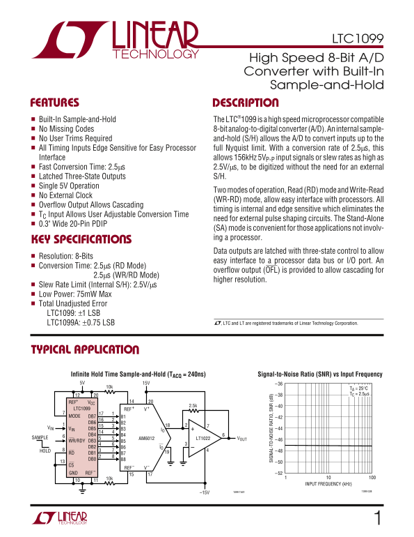
Page 1 Text Content
LTC1099
High Speed 8-Bit A/D Converter with Built-In Sample-and-Hold
FEATURES DESCRIPTIO Built-In Sample-and-Hold The LTC®1099 is a high speed microprocessor compatible No Missing Codes 8-bit analog-to-digital converter (A/D). An internal sample- No User Trims Required and-hold (S/H) allows the A/D to convert inputs up to the
All Timing Inputs Edge Sensitive for Easy Processor full Nyquist limit. With a conversion rate of 2.5µs, this Interface allows 156k Hz 5VP-P input signals or slew rates as high as
Fast Conversion Time: 2.5µs 2.5V/µs, to be digitized without the need for an external
Latched Three-State Outputs S/H.
Single 5V Operation
Two modes of operation, Read (RD) mode and Write-Read
No External Clock
(WR-RD) mode, allow easy interface with processors. All
Overflow Output Allows Cascading
timing is internal and edge sensitive which eliminates the
TC Input Allows User Adjustable Conversion Time
need for external pulse shaping circuits. The Stand-Alone
0.3" Wide 20-Pin PDIP
(SA) mode is convenient for those applications not involv- ing a processor.
KEY SPECIFICATIO S
Data outputs are latched with three-state control to allow
Resolution: 8-Bits
easy interface to a processor data bus or I/O port. An
Conversion Time: 2.5µs (RD Mode)
SI AL -T -N IS AT IO , S (d B) overflow output (OFL) is provided to allow cascading for
2.5µs (WR/RD Mode)
higher resolution.
Slew Rate Limit (Internal S/H): 2.5V/µs Low Power: 75m W Max Total Unadjusted Error LTC1099: ±1 LSB
LTC1099A: ±0.75 LSB , LTC and LT are registered trademarks of Linear Technology Corporation.
TYPICAL APPLICATION Infinite Hold Time Sample-and-Hold (TACQ = 240ns) Signal-to-Noise Ratio (SNR) vs Input Frequency
TA = 25°C –38 TC = 2.5µs
VCCREF+
LTC1099 REF+ MODE DB7 B1 –42 DB6 B2
VIN VIN DB5 B3 –44
DB4 B4
SAMPLE VOUTLT1022AM6012
WR/RDY DB3 –46
DB2 B6 IO
HOLD –48
RD DB1 B7 DB0 B8
GND REF –52
INPUT FREQUENCY (k Hz)
1099 TA01 1099 G08
Page Summary Contents For LINEAR TECHNOLOGY LTC1099 User's Manual
Manual Details
| Brand | Linear |
|---|---|
| Pages | 16 |
| File Size | 193.80 KB |
| Published | June 02, 2026 |
Enter the captcha to get the download link:

Frequently Asked Questions
What is the maximum conversion rate and slew rate supported?
The converter supports a high speed with a conversion time of 2.5ms, handling inputs up to 156kHz or slew rates as high as 2.5V/ms.
How can I achieve higher resolution for the measurement?
By utilizing the provided overflow output (OFL), you can implement cascading to achieve a higher effective resolution for 2.5ms conversion time.
What power and operating temperature range is specified for the device?
The typical maximum power dissipation is 75mW, and the operating temperature range varies by model; digital inputs support -40°C to 85°C in LTC1099AI/LTC1099AI.
Does it require external circuits or clocks for operation?
No, it features built-in Sample-and-Hold (S/H) and internal, edge-sensitive timing inputs, eliminating the need for external pulse shaping circuits or external clocks.