# A B C D E F G H I J K L M N O P Q R S T U V W X Y Z

LINEAR TECHNOLOGY LTC2499 Data Sheet / Manual

Summary

This advanced 24-bit, 16-channel Analog-to-Digital Converter (ADC) is designed for high-precision data acquisition systems requiring superior accuracy and low noise performance. Featuring patented Easy Drive technology and a direct sensor digitizer, it supports high impedance sensors while maintaining exceptional DC linearity and operating in single supply mode. The integrated temperature sensor provides comprehensive monitoring capability. This technical manual offers engineers detailed electrical specifications, absolute maximum ratings, and operational guidelines necessary for integrating the device into industrial process control or scientific instrumentation applications.
📄 Preview PAGE OF 32

Page 1 Text Content

LTC2499

24-Bit 8-/16-Channel

DS ADC with Easy Drive Input Current Cancellation and I2C Interface

Fea Tures Descrip Tion ■ Up to Eight Differential or 16 Single-Ended Inputs

The LTC®2499 is a 16-channel (eight differential), 24-bit,

■ Easy Drive TM Technology Enables Rail-to-Rail

No Latency DSTM ADC with Easy Drive technology and a

Inputs with Zero Differential Input Current 2-wire, I2C interface. The patented sampling scheme elimi- ■ Directly Digitizes High Impedance Sensors with

nates dynamic input current errors and the shortcomings

Full Accuracy of on-chip buffering through automatic cancellation of ■ 2-Wire I2C Interface with 27 Addresses Plus One

differential input current. This allows large external source

Global Address for Synchronization impedances and rail-to-rail input signals to be directly ■ 600n V RMS Noise

digitized while maintaining exceptional DC accuracy.

■ Integrated High Accuracy Temperature Sensor

The LTC2499 includes a high accuracy, temperature

■ GND to VCC Input/Reference Common Mode Range

sensor and an integrated oscillator. This device can be

■ Programmable 50Hz, 60Hz or Simultaneous 50Hz/

configured to measure an external signal (from combi-

60Hz Rejection Mode

nations of 16 analog input channels operating in single-

■ 2ppm INL, No Missing Codes

ended or differential modes) or its internal temperature

■ 1ppm Offset and 15ppm Full-Scale Error

sensor. The integrated temperature sensor offers 1/30th

■ 2x Speed/Reduced Power Mode (15Hz Using Internal

°C resolution and 2°C absolute accuracy.

Oscillator and 80µA at 7.5Hz Output) AB SO LU TE RR OR (° C)

■ No Latency: Digital Filter Settles in a Single Cycle, The LTC2499 allows a wide common mode input range

Even After a New Channel Is Selected (0V to VCC), independent of the reference voltage. Any

■ Single Supply 2.7V to 5.5V Operation (0.8m W) combination of single-ended or differential inputs can ■ Internal Oscillator be selected and the first conversion, after a new channel ■ Tiny 5mm × 7mm QFN Package is selected, is valid. Access to the multiplexer output en-

ables optional external amplifiers to be shared between all applica Tions analog inputs and auto calibration continuously removes their associated offset and drift.

■ Direct Sensor Digitizer

, LT, LTC and LTM are registered trademarks of Linear Technology Corporation.

■ Direct Temperature Measurement

No Latency DS and Easy Drive are trademarks of Linear Technology Corporation. All other trademarks are the property of their respective owners.

■ Instrumentation

■ Industrial Process Control

Typical applica Tion

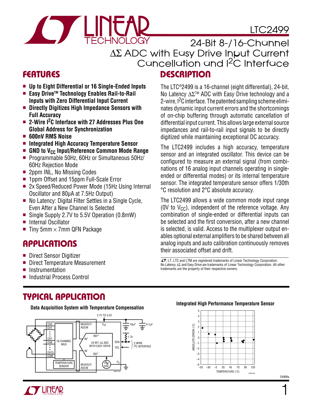
Integrated High Performance Temperature Sensor

Data Acquisition System with Temperature Compensation

2.7V TO 5.5V

CH0 VCCMUXOUT/ 10µF 0.1µF

CH1 ADCIN

REF+ 1.7k

CH7 IN+ 16-CHANNEL SDA CH8 24-BIT ∆Σ ADC 2-WIRE –1

WITH EASY DRIVE I2C INTERFACE

REF –3

TEMPERATURE FO

MUXOUT/ –5

SENSOR OSC

ADCIN –55 –30 –5

2499 TA01 TEMPERATURE (°C)

2499 TA02

2499fa

Page Summary Contents For LINEAR TECHNOLOGY LTC2499 Data Sheet / Manual

Page 1 LTC2499 24-Bit 8-/16-Channel DS ADC with Easy Drive Input Current Cancellation and I2C Interface Fea Tures Descrip Tion ■ Up to Eight Differential or 16 Single-Ended Inputs The LTC®2499 is a 16-channe...
Page 2 LTC2499 package/or Der in Forma Tionabsolu Te maximum ra Tings (Notes 1, 2) TOP VIEW Supply Voltage (VCC) ................................... –0.3V to 6V Analog Input Voltage (CH0-CH15, COM) ............
Page 3 LTC2499 elec Trical charac Teris Tics (normal spee D) The ● denotes the specifications which apply over the full operating temperature range, otherwise specifications are at TA = 25°C. (Notes 3, 4) PA...
Page 4 LTC2499 analog inpu T an D re Ference The ● denotes the specifications which apply over the full operating temperature range, otherwise specifications are at TA = 25°C. (Note 3) SYMBOL PARAMETER CONDI...
Page 5 LTC2499 power requiremen Ts The ● denotes the specifications which apply over the full operating temperature range, otherwise specifications are at TA = 25°C. (Note 3) SYMBOL PARAMETER CONDITIONS MIN ...
Page 6 NU BE OF EA DI NG TU (p pm f V RE F) IN (p pm f V RE F) LTC2499 Typical per Formance charac Teris Tics Integral Nonlinearity Integral Nonlinearity Integral Nonlinearity (VCC = 5V, VREF = 5V) (VCC = 5V...
Page 7 OF FS ET RR OR (p pm f V RM NO IS (µ V) RM NO IS (µ V) RE F) LTC2499 Typical per Formance charac Teris Tics RMS Noise vs Input Differential Voltage RMS Noise vs VIN(CM) RMS Noise vs Temperature (TA) 1...
Page 8 RE JE CT IO (d B) SL EE OD CU RR EN (µ A) FR EQ UE NC (k Hz LTC2499 Typical per Formance charac Teris Tics On-Chip Oscillator Frequency On-Chip Oscillator Frequency vs Temperature vs VCC PSRR vs Frequ...
Page 9 RM NO IS (µ V) IN (p pm EF LTC2499 Typical per Formance charac Teris Tics Integral Nonlinearity (2x Speed Integral Nonlinearity (2x Speed Noise Histogram Mode; VCC = 5V, VREF = 2.5V) Mode; VCC = 2.7V,...
Page 10 OF FS ET RR OR (µ V) LTC2499 Typical per Formance charac Teris Tics RR EJ EC TI ON (d B) Offset Error vs VCC Offset Error vs VREF PSRR vs Frequency at VCC (2x Speed Mode) (2x Speed Mode) (2x Speed Mod...
Page 11 LTC2499 pin Func Tions NC (Pin 5): No Connect. This pin can be left floating or VCC (Pin 28): Positive Supply Voltage. Bypass to GND with tied to GND. a 10µF tantalum capacitor in parallel with a 0.1µ...
Page 12 LTC2499 applica Tions in Forma Tion CONVERTER OPERATION POWER-ON RESET DEFAULT CONFIGURATION: IN+ = CH0, IN– = CH1 Converter Operation Cycle 50Hz/60Hz REJECTION 1X OUTPUT The LTC2499 is a multichannel...
Page 13 LTC2499 applica Tions in Forma Tion cancellation does not interfere with the transparent offset Input Voltage Range and full-scale auto-calibration and the absolute accuracy The analog inputs are trul...
Page 14 LTC2499 applica Tions in Forma Tion I2C INTERFACE finished, a Stop (P) condition is generated by transitioning SDA from low to high while SCL is high. The bus is free The LTC2499 communicates through ...
Page 15 LTC2499 applica Tions in Forma Tion The LTC2499 has two registers. The output register (32 are HIGH, the differential input voltage is equal to or above bits long) contains the last conversion result....
Page 16 LTC2499 applica Tions in Forma Tion INPUT DATA FORMAT If the first three bits are 000 or 100, the following data is ignored (don’t care) and the previously selected input The serial input word to the ...
Page 17 LTC2499 applica Tions in Forma Tion Table 3. Channel Selection MUX ADDRESS CHANNEL SELECTION ODD/ SGL SIGN A2 A1 A0 COM *0 IN+ IN– IN+ IN– IN+ IN– IN+ IN– IN+ IN– IN+ IN– IN+ IN– IN+ IN– IN– IN+ IN– I...
Page 18 LTC2499 applica Tions in Forma Tion The first bit of the second word is the enable bit for the up to 15Hz with no latency). When IM = 1 (temperature conversion configuration (EN2). If this bit is set ...
Page 19 LTC2499 DA TA OU applica Tions in Forma Tion Speed Mode (SPD) (see Figures 4 and 5). Slope calibration is not required if the reference voltage (VREF) is known. A 5V reference has Every conversion cyc...
Page 20 LTC2499 applica Tions in Forma Tion Initiating a New Conversion Table 5. Address Assignment CA2 CA1 CA0 ADDRESS When the LTC2499 finishes a conversion, it automatically enters the sleep state. Once in...
Page 21 LTC2499 applica Tions in Forma Tion 7-BIT ADDRESS R/W ACK DATA Sr DATA TRANSFERRING SLEEP DATA INPUT/OUTPUT CONVERSIONCONVERSION Figure 6. Conversion Sequence 7-BIT ADDRESS SR 7-BIT ADDRESSS RACK ACKR...
Page 22 LTC2499 applica Tions in Forma Tion 32 bits are read out of the device or after a Stop command. Synchronizing Multiple LTC2499s with a Global The following conversion will be performed using the Addre...
Page 23 LTC2499 applica Tions in Forma Tion to synchronize multiple converters without changing For many applications, the sensor output impedance the channel or configuration, a Stop may be issued after comb...
Page 24 LTC2499 applica Tions in Forma Tion input impedances, the common mode input current effects source impedances are not possible. One pair of external are rejected by the large CMRR of the LTC2499, lead...
Page 25 LTC2499 applica Tions in Forma Tion +F ER RO (p pm +F ER RO (p pm Reference Current for reference impedances of many k W (if CREF = 100p F up to 10k W will not degrade the performance (see Figures Sim...
Page 26 LTC2499 IN (p pm EF applica Tions in Forma Tion VCC = 5V When using the internal oscillator, the LTC2499 is de- VREF = 5V R = 1k signed to reject line frequencies. As shown in Figure VIN(CM) = 2.5V TA...
Page 27 LTC2499 applica Tions in Forma Tion The user can expect to achieve this level of performance modulator resolves this problem and guarantees stability using the internal oscillator, as shown in Figures...
Page 28 NO RM AL OD RE JE CT IO (d B) NO RM AL OD RE JE CT IO (d B) LTC2499 applica Tions in Forma Tion VCC = 5V VCC = 5V MEASURED DATA MEASURED DATA VREF = 5V VREF = 5V CALCULATED DATA CALCULATED DATA –20 VI...
Page 29 LTC2499 applica Tions in Forma Tion IN PU NO RM AL EJ EC TI ON (d B) Using the 2X speed mode of the LTC2499 alters the and effective resolution as well as a shift in frequency rejec- rejection charact...
Page 30 –F ER RO (p pm EF NO RM AL OD RE JE CT IO (d B) OF FS ET RR OR (p pm EF LTC2499 applica Tions in Forma Tion –70 VIN(CM) = VREF(CM) VIN(CM) = VREF(CM) VCC = VREF = 5V VCC = VREF = 5V VIN = 0V FO = EXT ...
Page 31 LTC2499 package Descrip Tion UHF Package 38-Lead Plastic QFN (5mm × 7mm) (Reference LTC DWG # 05-08-1701) 5.50 ± 0.05 (2 SIDES) 4.10 ± 0.05 (2 SIDES) 3.15 ± 0.05 (2 SIDES) PACKAGE OUTLINE 0.25 ± 0.05 ...
Page 32 LTC2499 Typical applica Tion External Buffers Provide High Impedance Inputs and Amplifier Offsets are Automatically Cancelled LTC2499 ∆Σ ADC ANALOG INPUT WITH INPUTS MUX EASY DRIVE SCL INPUTS 1/2 LTC6...

Manual Details

Brand Linear
Pages 32
File Size 606.58 KB
Published July 15, 2026
1 views

Enter the captcha to get the download link:

captcha

Frequently Asked Questions

What is the noise floor of the LTC2499 ADC?

It offers a low noise of 600nV RMS.

How does the device handle offset and drift?

Auto calibration continuously removes associated offset and drift from the input signals.

What kind of interfacing features are available for synchronization?

It utilizes a 2-wire I²C interface with up to 27 global addresses for synchronization.

Does the unit have precise temperature measurement capabilities?

Yes, it includes a high accuracy integrated temperature sensor with 1/30th °C resolution and 2°C absolute accuracy.