LINEAR TECHNOLOGY LTC2606 Data Sheet User Guide Manual
Summary
These single Rail-to-Rail Digital-to-Analog Converters (DACs) offer high precision across 16-, 14-, and 12-bit resolutions for applications requiring stable voltage output from a wide supply range (2.7V to 5.5V). Designed with low power consumption and built-in I²C serial interface compatibility, the LTC series ensures monotonic operation and excellent accuracy in challenging environments. This manual provides comprehensive technical specifications, electrical characteristics, and detailed application guidelines for engineers developing advanced systems in mobile communication, industrial automation, and instrumentation fields.
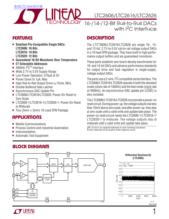
Page 1 Text Content
查询LTC2606供应商
LTC2606/LTC2616/LTC2626 16-/14-/12-Bit Rail-to-Rail DACs with I2C Interface FEATURES DESCRIPTIO
Smallest Pin-Compatible Single DACs: The LTC®2606/LTC2616/LTC2626 are single 16-, 14- LTC2606: 16 Bits and 12-bit, 2.7V-to-5.5V rail-to-rail voltage output DACs LTC2616: 14 Bits in a 10-lead DFN package. They have built-in high perfor- LTC2626: 12 Bits mance output buffers and are guaranteed monotonic. Guaranteed 16-Bit Monotonic Over Temperature
These parts establish new board-density benchmarks for
27 Selectable Addresses
16- and 14-bit DACs and advance performance standards
400k Hz I2CTM Interface
for output drive and load regulation in single-supply,
Wide 2.7V to 5.5V Supply Range
voltage-output DACs.
Low Power Operation: 270µA at 3V
Power Down to 1µA, Max The parts use a 2-wire, I2C compatible serial interface. The High Rail-to-Rail Output Drive (±15m A, Min) LTC2606/LTC2616/LTC2626 operate in both the standard Double-Buffered Data Latches mode (clock rate of 100k Hz) and the fast mode (clock rate Asynchronous DAC Update Pin of 400k Hz). An asynchronous DAC update pin (LDAC) is LTC2606/LTC2616/LTC2626: Power-On Reset to also included.
Zero Scale
The LTC2606/LTC2616/LTC2626 incorporate a power-on
LTC2606-1/LTC2616-1/LTC2626-1: Power-On Reset
reset circuit. During power-up, the voltage outputs rise less
to Midscale
than 10m V above zero scale; and after power-up, they stay
Tiny (3mm × 3mm) 10-Lead DFN Package
at zero scale until a valid write and update take place. The power-on reset circuit resets the LTC2606-1/LTC2616-1/
APPLICATIO DN (L SB
LTC2626-1 to midscale. The voltage outputs stay at midscale until a valid write and update take place.
Mobile Communications
Process Control and Industrial Automation , LTC and LT are registered trademarks of Linear Technology Corporation. All other trademarks are the property of their respective owners.
Instrumentation Automatic Test Equipment
BLOCK DIAGRA
Differential Nonlinearity
VCC REF
(LTC2606)
SCL 1.0
VOUT VCC = 5V
INPUT DAC
16-BIT DAC 0.8 VREF = 4.096V7
REGISTER REGISTER
I2C INTERFACE 0.4
CONTROL LOGIC
ADDRESS
CA2 DECODE
LDAC GND CODE
2606 BD 2606 G02
Page Summary Contents For LINEAR TECHNOLOGY LTC2606 Data Sheet User Guide Manual
Manual Details
| Brand | Linear |
|---|---|
| Pages | 20 |
| File Size | 309.61 KB |
| Published | May 30, 2026 |
Enter the captcha to get the download link:

Frequently Asked Questions
What bit depth options are available for this series?
The chips come in 16-bit (LTC2606), 14-bit (LTC2616), and 12-bit (LTC2626) options.
How does the device handle power-up reset?
Upon power-up, outputs rise to less than 10mV above zero scale until a valid write and update take place. LTC2626-1 stays at midscale until this occurs.
What is the maximum clock rate for output updates?
The device supports both standard mode (100kHz) and fast mode (400kHz) operation.
What is the low power consumption draw?
The parts are designed for low power, consuming only 270µA at 3V in standard mode and can drop to 1µA in maximum power-down mode.