# A B C D E F G H I J K L M N O P Q R S T U V W X Y Z

LINEAR TECHNOLOGY - LTC2411 Data Sheet Manual User Guide

Summary

The LTC2411/LTC2411-1 is a high-precision, 24-Bit No Latency Delta-Sigma Analog-to-Digital Converter, ideal for demanding scientific and industrial measurement applications. This micropower ADC features differential inputs and reference capabilities, providing superior accuracy and deep rejection of line noise (50/60Hz). The manual details comprehensive technical specifications, operational guidelines, and diverse application field compatibility for users in data acquisition systems, including weight scales, gas analyzers, and process control instrumentation requiring stable, high-resolution readings.
📄 Preview PAGE OF 40

Page 1 Text Content

LTC2411/LTC2411-1

24-Bit No Latency ∆ΣTM ADC with Differential Input and

Reference in MSOP

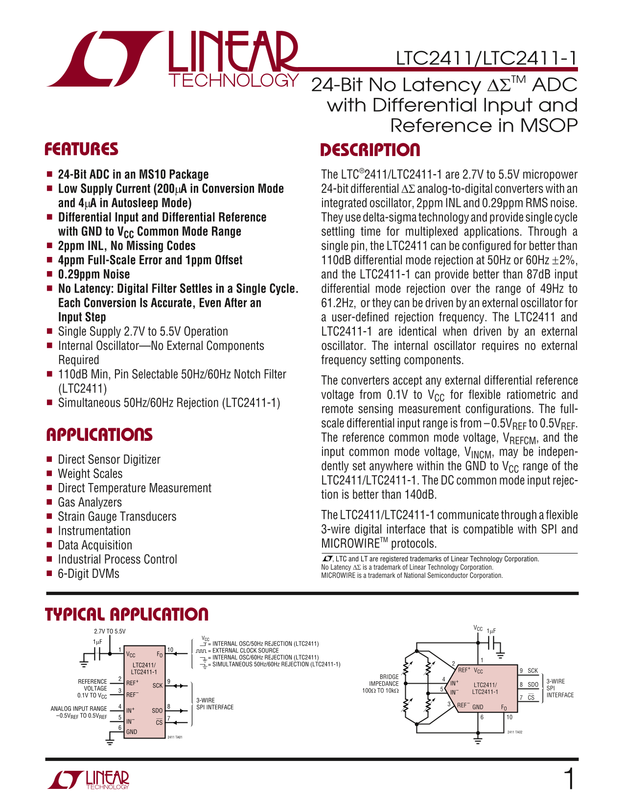
FEATURES DESCRIPTIO 24-Bit ADC in an MS10 Package The LTC®2411/LTC2411-1 are 2.7V to 5.5V micropower Low Supply Current (200µA in Conversion Mode 24-bit differential ∆Σ analog-to-digital converters with an and 4µA in Autosleep Mode) integrated oscillator, 2ppm INL and 0.29ppm RMS noise. Differential Input and Differential Reference They use delta-sigma technology and provide single cycle

with GND to VCC Common Mode Range settling time for multiplexed applications. Through a 2ppm INL, No Missing Codes single pin, the LTC2411 can be configured for better than 4ppm Full-Scale Error and 1ppm Offset 110d B differential mode rejection at 50Hz or 60Hz ±2%, 0.29ppm Noise and the LTC2411-1 can provide better than 87d B input No Latency: Digital Filter Settles in a Single Cycle. differential mode rejection over the range of 49Hz to Each Conversion Is Accurate, Even After an 61.2Hz, or they can be driven by an external oscillator for Input Step a user-defined rejection frequency. The LTC2411 and Single Supply 2.7V to 5.5V Operation LTC2411-1 are identical when driven by an external Internal Oscillator—No External Components oscillator. The internal oscillator requires no external Required frequency setting components.

110d B Min, Pin Selectable 50Hz/60Hz Notch Filter

The converters accept any external differential reference

(LTC2411)

voltage from 0.1V to VCC for flexible ratiometric and

Simultaneous 50Hz/60Hz Rejection (LTC2411-1)

remote sensing measurement configurations. The full- scale differential input range is from –0.5VREF to 0.5VREF.

APPLICATIO S The reference common mode voltage, VREFCM, and the

input common mode voltage, VINCM, may be indepen-

Direct Sensor Digitizer

dently set anywhere within the GND to VCC range of the

Weight Scales

LTC2411/LTC2411-1. The DC common mode input rejec-

Direct Temperature Measurement

tion is better than 140d B.

Gas Analyzers

Strain Gauge Transducers The LTC2411/LTC2411-1 communicate through a flexible Instrumentation 3-wire digital interface that is compatible with SPI and Data Acquisition MICROWIRETM protocols. Industrial Process Control , LTC and LT are registered trademarks of Linear Technology Corporation. No Latency ∆Σ is a trademark of Linear Technology Corporation.

6-Digit DVMs MICROWIRE is a trademark of National Semiconductor Corporation.

TYPICAL APPLICATIO

VCC 2.7V TO 5.5V 1µF

1µF = INTERNAL OSC/50Hz REJECTION (LTC2411)

= EXTERNAL CLOCK SOURCE

VCC FO

= INTERNAL OSC/60Hz REJECTION (LTC2411) LTC2411/ = SIMULTANEOUS 50Hz/60Hz REJECTION (LTC2411-1)

LTC2411-1 REF+ VCC SCK

BRIDGE

REFERENCE REF+ IN+ 3-WIRE

SCK IMPEDANCE LTC2411/ SDO

VOLTAGE SPI

100Ω TO 10kΩ IN– LTC2411-1

0.1V TO VCC REF– INTERFACE

3-WIRE

SPI INTERFACE REF GND FO

ANALOG INPUT RANGE IN+ SDO –0.5VREF TO 0.5VREF

IN– CS

GND 2411 TA02

2411 TA01

Page Summary Contents For LINEAR TECHNOLOGY - LTC2411 Data Sheet Manual User Guide

Page 1 LTC2411/LTC2411-1 24-Bit No Latency ∆ΣTM ADC with Differential Input and Reference in MSOP FEATURES DESCRIPTIO 24-Bit ADC in an MS10 Package The LTC®2411/LTC2411-1 are 2.7V to 5.5V micropower Low Supp...
Page 2 LTC2411/LTC2411-1 ABSOLUTE AXI U RATI GS PACKAGE/ORDER I FOR ATIO (Notes 1, 2) ORDER PART NUMBERSupply Voltage (VCC) to GND.......................–0.3V to 7V Analog Input Pins Voltage LTC2411CMS to GN...
Page 3 LTC2411/LTC2411-1 CO VERTER CHARACTERISTICS The ● denotes specifications which apply over the full operating temperature range, otherwise specifications are at TA = 25°C. (Notes 3, 4) PARAMETER CONDIT...
Page 4 LTC2411/LTC2411-1 DIGITAL I PUTS A D DIGITAL OUTPUTS The ● denotes specifications which apply over the full operating temperature range, otherwise specifications are at TA = 25°C. (Note 3) SYMBOL PARA...
Page 5 LTC2411/LTC2411-1 UW TI I G CHARACTERISTICS The ● denotes specifications which apply over the full operating temperature range, otherwise specifications are at TA = 25°C. (Note 3) SYMBOL PARAMETER CON...
Page 6 NU BE OF EA DI NG IN (p pm EF TU (p pm EF LTC2411/LTC2411-1 TYPICAL PERFOR A CE CHARACTERISTICS Total Unadjusted Error Total Unadjusted Error Total Unadjusted Error (VCC = 5V, VREF = 5V) (VCC = 5V, VR...
Page 7 OF FS ET RR OR (p pm EF RM NO IS (µ V) RM NO IS (µ V) LTC2411/LTC2411-1 TYPICAL PERFOR A CE CHARACTERISTICS RMS Noise vs VINCM RMS Noise vs Temperature RMS Noise vs VCC 1.60 1.60 1.60 VCC = 5V VIN = 0...
Page 8 RE JE CT IO (d B) RE JE CT IO (d B) FU LL -S CA LE RR OR (p pm EF LTC2411/LTC2411-1 TYPICAL PERFOR A CE CHARACTERISTICS +Full-Scale Error vs Temperature –Full-Scale Error vs Temperature –Full-Scale Er...
Page 9 OF FS ET RR OR (p pm CO NV ER SI ON UR RE NT (µ A) LTC2411/LTC2411-1 TYPICAL PERFOR A CE CHARACTERISTICS Conversion Current Conversion Current Sleep Mode Current vs Temperature vs Output Data Rate vs ...
Page 10 LTC2411/LTC2411-1 PI FU CTIO S the Sleep mode and remains in this low power state as internal pull-up is automatically activated in Internal Serial long as CS is HIGH. A LOW-to-HIGH transition on CS C...
Page 11 LTC2411/LTC2411-1 APPLICATIO S I FOR ATIO CONVERTER OPERATION Through timing control of the CS and SCK pins, the LTC2411/LTC2411-1 offer several flexible modes of op- Converter Operation Cycle eration...
Page 12 LTC2411/LTC2411-1 APPLICATIO S I FOR ATIO integrity of the conversion result and of the serial interface the overrange or the underrange condition using distinct mode selection. (See the 2-wire I/O se...
Page 13 LTC2411/LTC2411-1 APPLICATIO S I FOR ATIO above +FS. If both Bit 29 and Bit 28 are LOW, the Data is shifted out of the SDO pin under control of the serial differential input voltage is below –FS. cloc...
Page 14 LTC2411/LTC2411-1 APPLICATIO S I FOR ATIO As long as the voltage on the IN+ and IN– pins is maintained within the – 0.3V to (VCC + 0.3V) absolute maximum operating range, a conversion result is genera...
Page 15 LTC2411/LTC2411-1 APPLICATIO S I FOR ATIO Table 3. LTC2411/LTC2411-1 State Duration State Operating Mode Duration CONVERT Internal Oscillator FO = LOW (LTC2411) 133ms, Output Data Rate ≤ 7.5 Readings/...
Page 16 LTC2411/LTC2411-1 APPLICATIO S I FOR ATIO Table 4. LTC2411/LTC2411-1 Interface Timing Modes Conversion Data Connection SCK Cycle Output and Configuration Source Control Control Waveforms External SCK,...
Page 17 LTC2411/LTC2411-1 APPLICATIO S I FOR ATIO device automatically enters the low power sleep state once requiring all 32 bits of output data, aborting an invalid the conversion is complete. conversion cy...
Page 18 LTC2411/LTC2411-1 APPLICATIO S I FOR ATIO Data is shifted out the SDO pin on each falling edge of SCK Internal Serial Clock, Single Cycle Operation enabling external circuitry to latch data on the ris...
Page 19 LTC2411/LTC2411-1 APPLICATIO S I FOR ATIO In order to select the internal serial clock timing mode, the if the device is using its internal oscillator for the LTC2411 serial clock pin (SCK) must be fl...
Page 20 LTC2411/LTC2411-1 APPLICATIO S I FOR ATIO aborts the data output state and immediately initiates a A similar situation may occur during the sleep state when new conversion. This is useful for systems ...
Page 21 LTC2411/LTC2411-1 APPLICATIO S I FOR ATIO The internal serial clock mode is selected at the end of the The digital output signals (SDO and SCK in Internal SCK power-on reset (POR) cycle. The POR cycle...
Page 22 LTC2411/LTC2411-1 APPLICATIO S I FOR ATIO Particular attention must be given to the connection of the Driving the Input and Reference FO signal when the LTC2411/LTC2411-1 are used with an The input an...
Page 23 LTC2411/LTC2411-1 APPLICATIO S I FOR ATIO a 13µs (14.2µs) sampling period. Thus, for settling errors they include the effect of the actual second order input of less than 1ppm, the driving source impe...
Page 24 LTC2411/LTC2411-1 +F ER RO (p pm EF APPLICATIO S I FOR ATIO Larger values of input capacitors (CIN > 0.01µF) may be reference common mode voltages. While the input drive required in certain configu...
Page 25 LTC2411/LTC2411-1 OF FS ET RR OR (p pm EF APPLICATIO S I FOR ATIO does not change the converter offset, but it may degrade VCC = 5V REF+ = 5V – = GND the gain and INL performance. The effect of this c...
Page 26 LTC2411/LTC2411-1 +F ER RO (p pm EF +F ER RO (p pm EF APPLICATIO S I FOR ATIO VCC = 5V VCC = 5V REF+ = 5V REF+ = 5V – = GND – = GND REF REF IN+ = 3.75V IN+ = 1.25V – = 1.25V – = 3.75V IN IN FO = GND F...
Page 27 LTC2411/LTC2411-1 APPLICATIO S I FOR ATIO user is thus advised to minimize the combined source accompanied by three potential effects, which must be impedance driving the REF+ and REF– pins rather tha...
Page 28 LTC2411/LTC2411-1 RE SO LU TI ON (B IT S) –F ER RO (p pm OF FS ET RR OR (p pm EF APPLICATIO S I FOR ATIO VCC = 5V VCC = 5V VREF = 5V VREF = 5V VINCM = 2.5V IN+ = 3.75V VIN = 0V IN FO = EXT OSC FO = EX...
Page 29 LTC2411/LTC2411-1 RE SO LU TI ON (B IT S) APPLICATIO S I FOR ATIO VREF = 5V VREF = 2.5V VREF = 5VVREF = 2.5V VCC = 5V VCC = 5V REF– = GND REF– = GND VINCM = 2.5V VINCM = 2.5V VIN = 0V VIN = 0V FO = EX...
Page 30 LTC2411/LTC2411-1 PU RE FE RR ED OI SE IN PU NO RM AL OD RE JE CT IO (d B) EQ UI VA LE NT AN DW ID TH (H z) APPLICATIO S I FOR ATIO internal calibration and filtering. The noise of the driving noise f...
Page 31 LTC2411/LTC2411-1 IN PU NO RM AL OD RE JE CT IO (d B) APPLICATIO S I FOR ATIO INPUT SIGNAL FREQUENCY (Hz) INPUT SIGNAL FREQUENCY (Hz) Figure 32. Input Normal Mode Rejection Figure 33. Input Normal Mod...
Page 32 LTC2411/LTC2411-1 NO RM AL OD RE JE CT IO (d B) APPLICATIO S I FOR ATIO MEASURED DATA VCC = 5V VIN(P-P) = 5V VCC = 5V CALCULATED DATA VREF = 5V VIN(P-P) = 7.5V VREF = 5V –20 –20 (150% OF FULL SCALE) V...
Page 33 LTC2411/LTC2411-1 APPLICATIO S I FOR ATIO Averaging 64 samples however reduces the noise level by Another option is the use of a reference within the 5V input a factor of eight, bringing the resolving...
Page 34 LTC2411/LTC2411-1 APPLICATIO S I FOR ATIO the sensor largely eliminates the need for protection input stage from the transient load steps produced during devices, RFI suppression and wiring. The LTC24...
Page 35 LTC2411/LTC2411-1 APPLICATIO S I FOR ATIO Note that this 4-amplifier topology has advantages over Common mode gain is half the differential gain. The the typical integrated 3-amplifier instrumentation...
Page 36 LTC2411/LTC2411-1 APPLICATIO S I FOR ATIO bridge output can be eliminated completely; if the refer- result as the two resistor version, but has a few benefits. ence arm of the bridge is used as the re...
Page 37 LTC2411/LTC2411-1 APPLICATIO S I FOR ATIO 15VU1 LTC1043 LT1236-5 10V LTC1150 BRIDGE VCC LTC2411/ LTC2411-1 REF+ LTC1043 LTC1150 *FLYING CAPACITORS ARE 1µF FILM (MKP OR EQUIVALENT) LTC1043 SEE LTC1043 ...
Page 38 LTC2411/LTC2411-1 APPLICATIO S I FOR ATIO gain error or due to offset voltages. A 1µV/°C offset voltage the LTC2411/LTC2411-1 of 2.5V, maximizing the AC input drift translates into 0.05ppm/°C gain err...
Page 39 LTC2411/LTC2411-1 PACKAGE DESCRIPTIO MS10 Package 10-Lead Plastic MSOP (Reference LTC DWG # 05-08-1661) 0.043 0.034 (1.10) (0.86) MAX REF 0° – 6° TYP SEATING PLANE MSOP (MS10) 1100 (0.50) BSC DIMENSIO...
Page 40 LTC2411/LTC2411-1 TYPICAL APPLICATIO 5V LT1236-5 2N3904 LT1112 RN1 10k 10k VCC 350Ω BRIDGE LTC2411/ TWO ELEMENTS LTC2411-1 VARYING RN1 RN1 GND 10k 10k 0.1µF RN1 IS CADDOCK T914 10K-010-02 Q2, Q3 20Ω 1...

Manual Details

Brand Linear
Pages 40
File Size 1015.13 KB
Published July 22, 2026
0 views

Enter the captcha to get the download link:

captcha

Frequently Asked Questions

What is the input voltage range for the LTC2411/LTC2411-1?

The differential analog input range is –0.5V to 0.5V.

Does this ADC require an external oscillator?

No, it features an integrated oscillator and requires no external components for basic function.

How can I set the frequency rejection for power lines?

It offers selectable notch filters for simultaneous 50Hz/60Hz rejection (LTC2411-1) or a user-defined external frequency on LTC2411.

What voltage range does it operate within?

The device operates using a single supply of 2.7V to 5.5V.