# A B C D E F G H I J K L M N O P Q R S T U V W X Y Z

LINEAR TECHNOLOGY - 1 LTC1148 Data Sheet

Summary

The LTC1148 series are ultrahigh-efficiency synchronous step-down switching regulators engineered for portable and battery-powered electronics. Offering over 95% efficiency even at low load currents, these controllers utilize current-mode operation and adaptive Burst Mode to minimize power draw in applications like notebook computers, instruments, and digital devices. The manual provides comprehensive details on electrical specifications, wide input/dropout capabilities (up to 20V), protection features, and advanced circuit designs for electrical engineers designing reliable, low-power DC/DC systems.
📄 Preview PAGE OF 20

Page 1 Text Content

LTC1148

LTC1148-3.3/LTC1148-5 High Efficiency Synchronous

Step-Down Switching Regulators

FEATURES DESCRIPTIO Ultrahigh Efficiency: Over 95% Possible The LTC®1148 series is a family of synchronous step- Current-Mode Operation for Excellent Line and Load down switching regulator controllers featuring automatic Transient Response Burst Mode TM operation to maintain high efficiencies at High Efficiency Maintained Over Three Decades of low output currents. These devices drive external comple- Output Current mentary power MOSFETs at switching frequencies up to Low 160µA Standby Current at Light Loads 250k Hz using a constant off-time current-mode architec- Logic Controlled Micropower Shutdown: IQ < 20µA ture providing constant ripple current in the inductor. Wide VIN Range: 3.5V* to 20V

The operating current level is user-programmable via an

Short-Circuit Protection

external current sense resistor. Wide input supply range

Very Low Dropout Operation: 100% Duty Cycle

allows operation from 3.5V* to 18V (20V maximum).

Synchronous FET Switching for High Efficiency

Constant off-time architecture provides low dropout regu-

Adaptive Nonoverlap Gate Drives

lation limited by only the RDS(ON) of the external MOSFET

Output Can Be Externally Held High in Shutdown

and resistance of the inductor and current sense resistor.

Available in 14-Pin Narrow SO Package

The LTC1148 series combines synchronous switching for maximum efficiency at high currents with an automatic low

APPLICATIO S

current operating mode, called Burst Mode operation, which

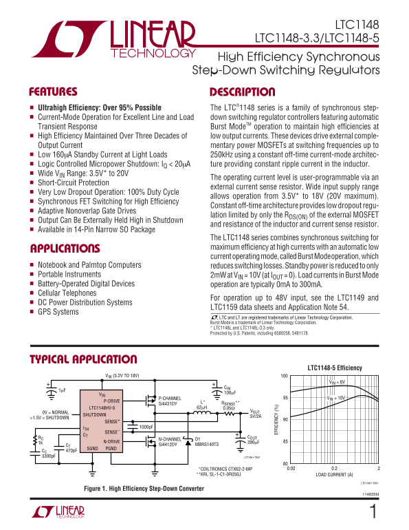
Notebook and Palmtop Computers reduces switching losses. Standby power is reduced to only Portable Instruments EF FI CI EN CY 2m W at VIN = 10V (at IOUT = 0). Load currents in Burst Mode Battery-Operated Digital Devices operation are typically 0m A to 300m A. Cellular Telephones

For operation up to 48V input, see the LTC1149 and

DC Power Distribution Systems

LTC1159 data sheets and Application Note 54.

GPS Systems

, LTC and LT are registered trademarks of Linear Technology Corporation. Burst Mode is a trademark of Linear Technology Corporation. * LTC1148L and LTC1148L-3.3 only. Protected by U.S. Patents, including 6580258, 5481178.

TYPICAL APPLICATIO

LTC1148-5 Efficiency

VIN (5.2V TO 18V)

VIN = 6V

P-CHANNEL VIN = 10V

P-DRIVE L*

Si4431DY RSENSE**

LTC1148HV-5 62µH 0.05Ω

0V = NORMAL

SHUTDOWN

>1.5V = SHUTDOWN

SENSE+

ITH 1000p F

SENSE–

RC COUT

N-CHANNEL D1

1k N-DRIVE 390µF

CT Si4412DY MBRS140T3

SGND PGND

470p FCC

3300p F LT1148 • TA01

COILTRONICS CTX62-2-MP 0.02 0.2

KRL SL-1-C1-0R050J LOAD CURRENT (A)

LTC1148 • TA01

Figure 1. High Efficiency Step-Down Converter

114835fd

Page Summary Contents For LINEAR TECHNOLOGY - 1 LTC1148 Data Sheet

Page 1 LTC1148 LTC1148-3.3/LTC1148-5 High Efficiency Synchronous Step-Down Switching Regulators FEATURES DESCRIPTIO Ultrahigh Efficiency: Over 95% Possible The LTC®1148 series is a family of synchronous step...
Page 2 LTC1148 LTC1148-3.3/LTC1148-5 XI ARBSOLUTE TI PACKAGE/ORDER FOR ATIO (Note 1) Input Supply Voltage (Pin 3) ORDER PART LTC1148 and LTC1148L Series 16V to –0.3V NUMBER TOP VIEW LTC1148HV Series 20V to –...
Page 3 LTC1148 LTC1148-3.3/LTC1148-5 ELECTRICAL CHARA TERISTICS The ● denotes the specifications which apply over the full operating temperature range, otherwise specifications are at TA = 25°C. VIN = 10V, V...
Page 4 LTC1148 SU PP LY UR RE NT (m A) EF FI CI EN CY LTC1148-3.3/LTC1148-5 ELECTRICAL CHARA TERISTICS Note 1: Absolute Maximum Ratings are those values beyond which the life Note 5: In applications where RS...
Page 5 LTC1148 GA TE HA RG CU RR EN (m A) LTC1148-3.3/LTC1148-5 PERFOR ATYPICAL CE CHARA TERISTICS Gate Charge Supply Current Off Time vs VOUT Current Sense Threshold Voltage – = VOUT VSENSE MAXIMUM THRESHOL...
Page 6 LTC1148 LTC1148-3.3/LTC1148-5 UU FU CTIO AL DIAGRA Pin 9 connection shown for LTC1148-3.3 and LTC1148-5; changes create LTC1148. P-DRIVE SGND SENSE+ SENSE– ADJUSTABLE VERSION VFB N-DRIVE SLEEP 25m V T...
Page 7 LTC1148 LTC1148-3.3/LTC1148-5 OPERATIO The LTC1148 series uses a current mode, constant off- (Pin 6) to increase the current comparator threshold, thus time architecture to synchronously switch an ext...
Page 8 LTC1148 LTC1148-3.3/LTC1148-5 APPLICATIO S I FOR ATIO The basic LTC1148 series application circuit (fixed 0.20 output versions) is shown in Figure 1. External compo- nent selection is driven by the lo...
Page 9 LTC1148 LTC1148-3.3/LTC1148-5 CA PA CI TA NC (p F) APPLICATIO S I FOR ATIO VSENSE– = VOUT = 5V Inductor Core Selection Once the minimum value for L is known, the type of inductor must be selected. The...
Page 10 LTC1148 LTC1148-3.3/LTC1148-5 APPLICATIO S I FOR ATIO level threshold MOSFETs (VGS(TH) &lt; 2.5V) are strongly CIN and COUT Selection recommended. The LTC1148/LTC1148HV series supply In continuous mod...
Page 11 LTC1148 LTC1148-3.3/LTC1148-5 WU UT (µ F) APPLICATIO S I FOR ATIO In surface mount applications multiple capacitors may several cycles to respond to a step in DC (resistive) load have to be paralleled...
Page 12 LTC1148 LTC1148-3.3/LTC1148-5 APPLICATIO S I FOR ATIO LTC1148 DC supply current is 160µA for no load, and increases proportionally with load up to a constant GATE CHARGE 1.6m A after the LTC1148 serie...
Page 13 LTC1148 LTC1148-3.3/LTC1148-5 APPLICATIO S I FOR ATIO and δP = δN = 0.007(63 – 25) = 0.27. The required RDS(ON) To prevent stray pickup a 100p F capacitor is suggested for each MOSFET can now be calcu...
Page 14 LTC1148 LTC1148-3.3/LTC1148-5 APPLICATIO S I FOR ATIO With the addition of R3, a current is generated through R1 INTVCC causing an offset of: FROM CROWBAR DETECT CIRCUIT (ACTIVE WHEN VGATE = VIN VN222...
Page 15 LTC1148 LTC1148-3.3/LTC1148-5 APPLICATIO S I FOR ATIO – and SENSE + leads routed together Board Layout Checklist 3. Are the SENSE with minimum PC trace spacing? The 1000p F capacitor When laying out t...
Page 16 LTC1148 LTC1148-3.3/LTC1148-5 TYPICAL APPLICATIO S VIN VIN 5.2V TO 18V 4V TO 18V CIN CIN 1/2 Si4532 100µF 1/2 Si4532 D1 100µF 25V MBRS140T3 25V MBRS140T3 1/2 Si4532 1/2 Si4532 P-DRIVE N-DRIVE P-DRIVE ...
Page 17 LTC1148 LTC1148-3.3/LTC1148-5 TYPICAL APPLICATIO S VIN VIN 3.5V TO 14V 5V MMSF3P02HD 100µF Si9803DY D1 MBRS140T3 20V MBRS140T3 MMSF5N02HD Si9804DY P-DRIVE N-DRIVE P-DRIVE N-DRIVE NC NC NC NC LTC1148L-...
Page 18 LTC1148 LTC1148-3.3/LTC1148-5 TYPICAL APPLICATIO S VIN 4V TO 14V CIN 100µF Si4435DY 20V P-DRIVE N-DRIVE NC NC 10V LTC1148 OS-CON VIN PGND L1 50µH CT SGND CT D1 390p F MBRS140T3 INTVCC SHUTDOWN SHUTDOW...
Page 19 LTC1148 LTC1148-3.3/LTC1148-5 PACKAGE DESCRIPTIO N Package 14-Lead PDIP (Narrow 0.300) (LTC DWG # 05-08-1510) .770* (19.558) MAX MIN .065 .008 – .015 (1.651) (0.203 – 0.381) TYP –0.3818.255( MIN (2.54...
Page 20 LTC1148 LTC1148-3.3/LTC1148-5 TYPICAL APPLICATION VIN 10V TO 18V 20k VIN = 10V VIN = 14V MUR110 N-CH D1 IRFZ44 1N5818 VN2222LL P-DRIVE N-DRIVE N-CH IRFZ44 NC NC 0.1 LTC1148HV-5 LOAD CURRENT (A) VIN PG...