# A B C D E F G H I J K L M N O P Q R S T U V W X Y Z

LINEAR TECHNOLOGY LTC3733 LTC3733-1 Data Sheet Manual

Summary

This advanced 3-Phase Synchronous Buck Controller is engineered for high-performance, current-sharing power delivery in demanding applications like servers, workstations, and high-end computing CPUs. The manual details a robust architecture featuring phase separation up to 530kHz and accurate Voltage ID (VID) support ranging from 0.8V to 1.55V. It provides comprehensive protection, including OPTI-LOOP compensation and short-circuit shutdown, ensuring maximum efficiency and stability for modern processors requiring massive power output.
📄 Preview PAGE OF 32

Page 1 Text Content

LTC3733/LTC3733-1 3-Phase, Buck

Controllers for AMD CPUs

FEATURES DESCRIPTIO 3-Phase Controller with Onboard MOSFET Drivers The LTC®3733 family are Poly Phase® synchronous step- Current Mode Control Ensures Current Sharing down switching regulator controllers that drive all Differential Amplifier Accurately Senses VOUT N-channel external power MOSFET stages in a phase-

±5% Output Current Matching Optimizes Thermal lockable, fixed frequency architecture. The 3-phase con- Performance and Size of Inductors and MOSFETs troller drives its output stages with 120° phase separation Reduced Input and Output Capacitance at frequencies of up to 530k Hz per phase to minimize the Supports Active Voltage Positioning RMS current dissipated by the ESR of both the input and VID Programmable Output Voltage from 0.8V to 1.55V output filter capacitors. The 3-phase technique effectively (AMD Opteron TM CPU) triples the fundamental frequency, improving transient 6-Phase, 90A to 120A Operation response while operating each phase at an optimal fre- Output Power Good Indicator with Adaptive Blanking quency for efficiency and ease of thermal design. Light 210k Hz to 530k Hz Per Phase, PLL, Fixed Frequency load efficiency is optimized by using a choice of output Synchronizable (LTC3733-1) stage shedding or Burst Mode technology.

PWM, Stage Shedding or Burst Mode® Operation

A differential amplifier provides true remote sensing of both

OPTI-LOOP® Compensation Minimizes COUT

the high and low sides of the output voltage at load points.

Adjustable Soft-Start Current Ramping

Soft-start and a defeatable, timed short-circuit shutdown

Short-Circuit Shutdown Timer with Defeat Option

protect the MOSFETs and the load. A foldback current

No_CPU Detection

circuit also provides protection for the external MOSFETs

36-Lead 0.209" SSOP and 38-Lead (5mm × 7mm) QFN

under short-circuit or overload conditions. An all-“1” VID APPLICATIO detector turns off the regulator after 1µs timeout. , LTC and LT are registered trademarks of Linear Technology Corporation. High Performance Notebook Computers Burst Mode, OPTI-LOOP and Poly Phase are registered trademarks of Linear Technology Corporation. AMD Opteron is a trademark of Advanced Micro Devices, Inc.

Servers, Desktop Computers and Workstations

TYPICAL APPLICATIO

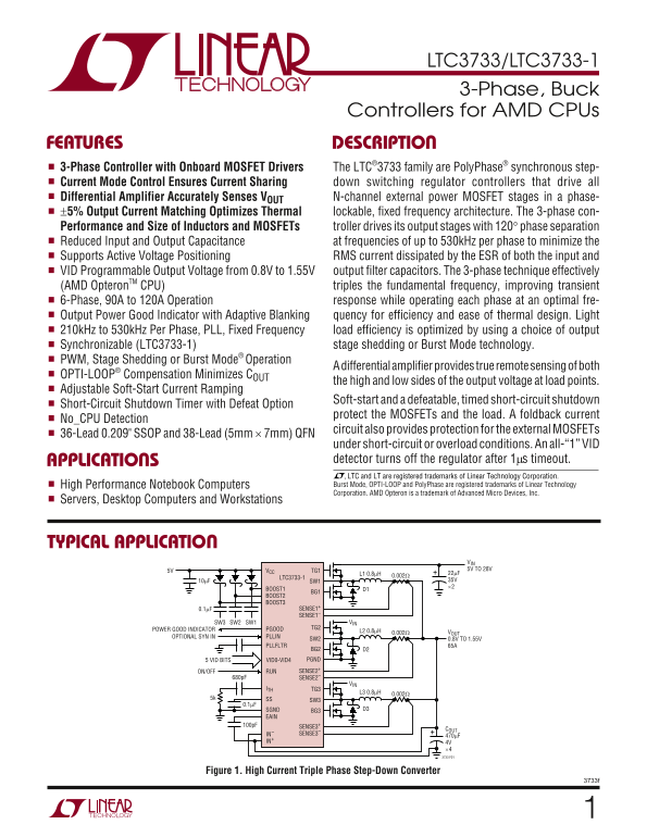
VIN 5V TG1VCC 5V TO 28V 22µF

LTC3733-1 0.002ΩL1 0.8µH

10µF SW1 35V ×2

BOOST1 D1

BOOST2 BOOST3

0.1µF SENSE1+ SENSE1–

SW3 SW2 SW1 VIN

POWER GOOD INDICATOR PGOOD TG2

0.002ΩL2 0.8µH VOUT

PLLINOPTIONAL SYN IN

SW2 0.8V TO 1.55V

PLLFLTR 65A

BG2 D2 5 VID BITS PGNDVID0-VID4

ON/OFF RUN SENSE2+

680p F SENSE2–

ITH TG3

5k SS

SGND BG3 D3

100p F SENSE3+

SENSE3–IN–

IN+ 4V

Figure 1. High Current Triple Phase Step-Down Converter

Page Summary Contents For LINEAR TECHNOLOGY LTC3733 LTC3733-1 Data Sheet Manual

Page 1 LTC3733/LTC3733-1 3-Phase, Buck Controllers for AMD CPUs FEATURES DESCRIPTIO 3-Phase Controller with Onboard MOSFET Drivers The LTC®3733 family are Poly Phase® synchronous step- Current Mode Control E...
Page 2 LTC3733/LTC3733-1 ABSOLUTE AXI U RATI GS (Note 1) Topside Driver Voltages (BOOSTN) 38V to –0.3V ITH Voltage 2.4V to –0.3V Switch Voltage (SWN)................................... 32V to –5V Operating A...
Page 3 LTC3733/LTC3733-1 ELECTRICAL CHARACTERISTICS The ● denotes the specifications which apply over the full operating temperature range, otherwise specifications are at TA = 25°C. VCC = VRUN = VSS = 5V un...
Page 4 LTC3733/LTC3733-1 ELECTRICAL CHARACTERISTICS The ● denotes the specifications which apply over the full operating temperature range, otherwise specifications are at TA = 25°C. VCC = VRUN = VSS = 5V un...
Page 5 FR EQ UE NC (k Hz RE FE RE NC VO LT AG (m V) EF FI CI EN CY LTC3733/LTC3733-1 TYPICAL PERFOR A CE CHARACTERISTICS Efficiency vs IOUT Efficiency vs VIN Efficiency vs Frequency VOUT = 1.5V VOUT = 1.5V V...
Page 6 PE AK EN SE OL TA GE (m V) SS UL L- UP UR RE NT (µ A) SS IN OL TA GE (V LTC3733/LTC3733-1 TYPICAL PERFOR A CE CHARACTERISTICS Short-Circuit Arming and Latchoff Shutdown Current vs vs Temperature Suppl...
Page 7 AX IM UM UR RE NT HR ES HO LD IS AT CH (m V) LTC3733/LTC3733-1 TYPICAL PERFOR A CE CHARACTERISTICS Maximum Current Threshold Shed Mode at 1Amp, Burst Mode at 1Amp, Mismatch vs Temperature Light Load C...
Page 8 LTC3733/LTC3733-1 PI FU CTIO S (G36/QFN) VID0 to VID4 (Pins 36, 1, 18, 19, 20/Pins 35, 36, 16, 17, SENSE1+, SENSE2+, SENSE3+, SENSE1–, SENSE2–, 18): Output Voltage Programming Input Pins. A 150k SENSE...
Page 9 LTC3733/LTC3733-1 PI FU CTIO S (G36/QFN) TG1 to TG3 (Pins 33, 30, 22/Pins 32, 29, 20): High PGOOD (Pin 35/Pin 34): This open-drain output is pulled Current Gate Drives for Top N-channel MOSFETs. These...
Page 10 LTC3733/LTC3733-1 FU CTIO AL DIAGRA PLLIN (LTC3733-1 ONLY) FIN PHASE DET RLP PLLFLTR OSCILLATOR CLK2 2.5µA VCC VIN FCB DUPLICATE FOR SECOND AND THIRD CONTROLLER CHANNELS BOOST DB PGOOD 0.66V CB OUT DE...
Page 11 LTC3733/LTC3733-1 OPERATIO (Refer to Functional Diagram) Main Control Loop forcing temporary forced PWM operation and 2) a logic input to select between three modes of operation. The IC uses a constan...
Page 12 LTC3733/LTC3733-1 OPERATIO (Refer to Functional Diagram) source or sink current in this mode. When forcing con- Short-Circuit Detection tinuous operation and sinking current, this current will be The ...
Page 13 LTC3733/LTC3733-1 OP ER AT IN FR EQ UE NC (k Hz APPLICATIO S I FOR ATIO The basic application circuit is shown in Figure 1 on the Inductor Value Calculation and Output Ripple Current first page of thi...
Page 14 LTC3733/LTC3733-1 APPLICATIO S I FOR ATIO So the number of phases used can be selected to minimize Ferrite designs have very low core loss and are preferred the output ripple current and therefore the...
Page 15 LTC3733/LTC3733-1 APPLICATIO S I FOR ATIO The power dissipation for the main and synchronous MILLER EFFECT MOSFETs at maximum output current are given by: OUT MAX MAIN DS ON CMILLER = (QB – QA)/VDS 37...
Page 16 LTC3733/LTC3733-1 APPLICATIO S I FOR ATIO δ = 0.005/°C can be used as an approximation for low So the phase number can be chosen to minimize the input voltage MOSFETs. capacitor size for the given inp...
Page 17 LTC3733/LTC3733-1 APPLICATIO S I FOR ATIO board trace and connector resistance losses are also with input voltage. The output ripple will be less than 50m V reduced by the reduction of the input rippl...
Page 18 LTC3733/LTC3733-1 APPLICATIO S I FOR ATIO series of surface-mount tantalums or the Panasonic SP to supply the high transient currents required by the series of surface mount special polymer capacitors...
Page 19 LTC3733/LTC3733-1 APPLICATIO S I FOR ATIO Output Voltage Table 1. VID Output Voltage Programming VID4 VID3 VID2 VID1 VID0 VOUT The IC includes a digitally controlled 5-bit attenuator producing output ...
Page 20 LTC3733/LTC3733-1 APPLICATIO S I FOR ATIO Fault Conditions: Overcurrent Latchoff to latch off the controller. Defeating this feature allows troubleshooting of the circuit and PC layout. The internal T...
Page 21 LTC3733/LTC3733-1 APPLICATIO S I FOR ATIO The emitter of Q1 will hold up the EAIN pin to a voltage in The output of the phase detector is a complementary pair the absence of VOUT that will prevent the...
Page 22 LTC3733/LTC3733-1 APPLICATIO S I FOR ATIO The loop filter components (CLP, RLP) smooth out the Efficiency Considerations current pulses from the phase detector and provide a The percent efficiency of ...
Page 23 LTC3733/LTC3733-1 APPLICATIO S I FOR ATIO The ITH series RC-CC filter sets the dominant pole-zero RSENSE resistor would require a 500µs rise time, limiting loop compensation. The values can be modifie...
Page 24 LTC3733/LTC3733-1 APPLICATIO S I FOR ATIO The output voltage will be set by the VID code according IC. These items are also illustrated graphically in the layout to Table 1. diagram of Figure 10. Chec...
Page 25 LTC3733/LTC3733-1 APPLICATIO S I FOR ATIO SW1 RSENSE1 L2 VOUT SW2 RSENSE2 CIN D2 COUT BOLD LINES INDICATE HIGH, SWITCHING CURRENT LINES. L3 KEEP LINES TO A MININMUM LENGTH SW3 RSENSE3 Figure 10. Branc...
Page 26 LTC3733/LTC3733-1 APPLICATIO S I FOR ATIO Figure 10 illustrates all branch currents in a three-phase finite impedances during the total period of the switching switching regulator. It becomes very cle...
Page 27 LTC3733/LTC3733-1 APPLICATIO S I FOR ATIO The worst-case input RMS ripple current for a single stage Efficiency Calculation design peaks at twice the value of the output voltage. The To estimate effic...
Page 28 LTC3733/LTC3733-1 APPLICATIO S I FOR ATIO The temperature of the MOSFET’s die temperature may Total of all three synchronous MOSFET’s AC loss: require interative calculations if one is not familiar ty...
Page 29 LTC3733/LTC3733-1 TYPICAL APPLICATIO 65A Power Supply for AMD Opteron Processors PGOOD VID1 IN VID1 VID0 VID0 IN ON/OFF RUN PGOOD PLLFLTR BOOST1 1Ω VIN 0.1µF VOUT FCB TG1 M1 L1 100p F IN+ SW1 LTC3733 ...
Page 30 LTC3733/LTC3733-1 PACKAGE DESCRIPTIO G Package 36-Lead Plastic SSOP (5.3mm) (Reference LTC DWG # 05-08-1640) 0.42 ±0.03 0.65 BSC RECOMMENDED SOLDER PAD LAYOUT BSC 0.05 NOTE: (.002) (.009 – .015) G36 S...
Page 31 LTC3733/LTC3733-1 PACKAGE DESCRIPTIO UHF Package 38-Lead Plastic QFN (7mm × 5mm) (Reference LTC DWG # 05-08-1701) 5.50 ± 0.05 (2 SIDES) 4.10 ± 0.05 (2 SIDES) 3.20 ± 0.05 (2 SIDES) PACKAGE OUTLINE 0.25...
Page 32 LTC3733/LTC3733-1 RELATED PARTS PART NUMBER DESCRIPTION COMMENTS LTC1628 2-Phase, Dual Output Synchronous Step-Down Reduces CIN and COUT, Power Good Output Signal, Synchronizable, DC/DC Controllers 3....

Manual Details

Brand Linear
Pages 32
File Size 285.96 KB
Published June 16, 2026
4 views

Enter the captcha to get the download link:

captcha

Frequently Asked Questions

What range of voltage does the programmable optimal output support?

The programmable output voltage (VID) can be set from 0.8V to 1.55V.

How does the three-phase technique improve performance?

It improves the transient response and allows each phase to operate at an optimal frequency, up to 530kHz per phase.

What safety protections are built into this controller?

Protection features include Short-Circuit Shutdown after a timed delay option, foldback current, and a detection circuit for external MOSFETs.

What is the required operating ambient temperature range?

The unit supports an operating ambient temperature range of 0°C to 70°C.