Page 1
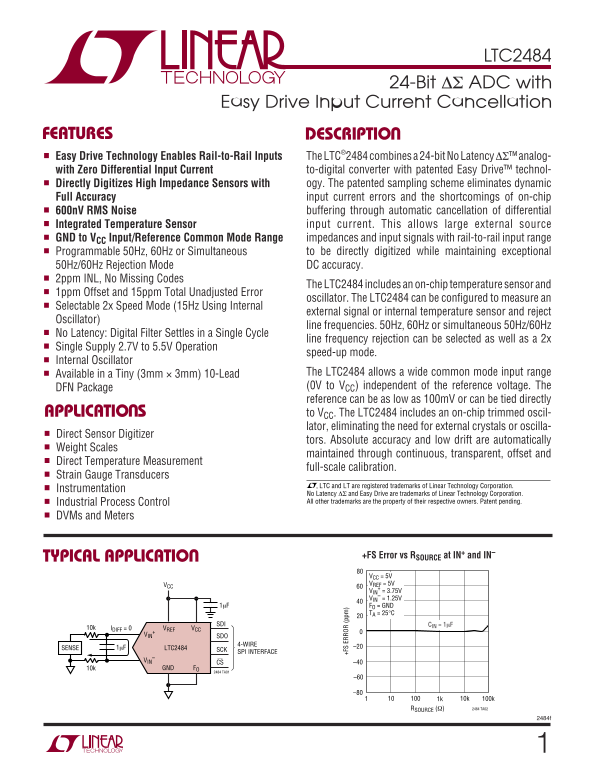
LTC2484 24-Bit ∆Σ ADC with Easy Drive Input Current Cancellation FEATURES DESCRIPTIO Easy Drive Technology Enables Rail-to-Rail Inputs The LTC®2484 combines a 24-bit No Latency ∆Σ™ analog- with Zero D...
Page 2
LTC2484 ABSOLUTE AXI U RATI GS PACKAGE/ORDER I FOR ATIO (Notes 1, 2) Supply Voltage (VCC) to GND...................... –0.3V to 6V TOP VIEW ORDER PART Analog Input Voltage to GND –0.3V to (VCC + 0.3V)...
Page 3
LTC2484 ELECTRICAL CHARACTERISTICS (2x SPEED) The ● denotes specifications which apply over the full operating temperature range, otherwise specifications are TA = 25°C. (Notes 3, 4) PARAMETER CONDITI...
Page 4
LTC2484 ALOG I PUT A D REFERE CE The ● denotes specifications which apply over the full operating temperature range, otherwise specifications are at TA = 25°C. (Note 3) SYMBOL PARAMETER CONDITIONS MIN...
Page 5
LTC2484 TI G CHARACTERISTICS The ● denotes specifications which apply over the full operating temperature range, otherwise specifications are at TA = 25°C. (Note 3) SYMBOL PARAMETER CONDITIONS MIN TYP...
Page 6
NU BE OF EA DI NG TU (p pm IN (p pm EF EF LTC2484 TYPICAL PERFOR A CE CHARACTERISTICS Integral Nonlinearity Integral Nonlinearity Integral Nonlinearity (VCC = 5V, VREF = 5V) (VCC = 5V, VREF = 2.5V) (V...
Page 7
OF FS ET RR OR (p pm RM NO IS (µ V) RM NO IS (p pm EF EF LTC2484 TYPICAL PERFOR A CE CHARACTERISTICS RMS Noise vs Input Differential Voltage RMS Noise vs VIN(CM) RMS Noise vs Temperature (TA) 1.0 1.0 ...
Page 8
RE JE CT IO (d B) FR EQ UE NC (k Hz TA T/ EF (V LTC2484 TYPICAL PERFOR A CE CHARACTERISTICS Temperature Sensor Temperature Sensor Error On-Chip Oscillator Frequency vs Temperature vs Temperature vs Te...
Page 9
IN (p pm SU PP LY UR RE NT (µ A) LTC2484 TYPICAL PERFOR A CE CHARACTERISTICS OF FS ET RR OR (µ V) Conversion Current Integral Nonlinearity (2x Speed Integral Nonlinearity (2x Speed vs Output Data Rate...
Page 10
OF FS ET RR OR (µ V) LTC2484 TYPICAL PERFOR A CE CHARACTERISTICS RR EJ EC TI ON (d B) Offset Error vs VCC Offset Error vs VREF PSRR vs Frequency at VCC (2x Speed Mode) (2x Speed Mode) (2x Speed Mode) ...
Page 11
LTC2484 PI FU CTIO S as CS is HIGH. A LOW-to-HIGH transition on CS during the Input/Output period. In External Serial Clock Operation Data Output transfer aborts the data transfer and starts a mode, S...
Page 12
LTC2484 TI I G DIAGRA S Timing Diagram Using Internal SCK t KQMIN t KQMAX 2484 TD1 SLEEP CONVERSIONDATA IN/OUT Timing Diagram Using External SCK UU WU t5 t KQMIN t6 t KQMAX t4 2484 TD2 SLEEP CONVERSIO...
Page 13
LTC2484 APPLICATIO S I FOR ATIO While in this sleep state, power consumption is reduced by network transparently removes the differential input cur- two orders of magnitude. The part remains in the sl...
Page 14
LTC2484 APPLICATIO S I FOR ATIO CS SUB LSBs BIT 31 BIT 29 BIT 28 BIT 27 BIT 26 BIT 4BIT 5 BIT 3 BIT 1 BIT 0BIT 2BIT 30 SDO EOC SIGDMY MSB LSB24 Hi-Z CONVERSION RESULT SDI EN DON’T CARE IM FOBFOA SPD D...
Page 15
LTC2484 APPLICATIO S I FOR ATIO Temperature Sensor (IM) Linearity, full-scale accuracy, full-scale drift are identical for both 2x and 1x speed modes. In both the 1x and 2x speed The LTC2484 includes ...
Page 16
LTC2484 APPLICATIO S I FOR ATIO Bit 28 (fourth output bit) is the most significant bit (MSB) In order to shift the conversion result out of the device, CS of the result. This bit in conjunction with B...
Page 17
LTC2484 APPLICATIO S I FOR ATIO Conversion Clock While operating with an external conversion clock of a frequency f EOSC, the LTC2484 provides better than 110d B A major advantage the delta-sigma conv...
Page 18
LTC2484 APPLICATIO S I FOR ATIO Table 4. LTC2484 State Duration STATE OPERATING MODE DURATION CONVERT Internal Oscillator 60Hz Rejection 133ms, Output Data Rate ≤ 7.5 Readings/s for 1x Speed Mode 67ms...
Page 19
LTC2484 TA (m V) APPLICATIO S I FOR ATIO When using the internal temperature sensor, if the output Reference Voltage Range code is normalized to RSDO = VPTAT/VREF, the temperature The LTC2484 external...
Page 20
LTC2484 APPLICATIO S I FOR ATIO SERIAL INTERFACE TIMING MODES When the device is in the sleep state, its conversion result is held in an internal static shift register. The device The LTC2484’s 4-wire...
Page 21
LTC2484 APPLICATIO S I FOR ATIO 2.7V TO 5.5V 1µF VCC FO INT/EXT CLOCK LTC2484 1REFERENCE VREF SDI VOLTAGE 0.1V TO VCC SCK 4-WIRE SPI INTERFACE ANALOG IN+ CS TEST EOC INPUT IN– GND (OPTIONAL) TEST EOC ...
Page 22
LTC2484 APPLICATIO S I FOR ATIO External Serial Clock, 3-Wire I/O each falling edge of SCK. EOC can be latched on the first rising edge of SCK. On the 32nd falling edge of SCK, This timing mode utiliz...
Page 23
LTC2484 APPLICATIO S I FOR ATIO When testing EOC, if the conversion is complete (EOC = 0), used to shift the conversion result into external circuitry. the device will exit the low power mode during t...
Page 24
LTC2484 APPLICATIO S I FOR ATIO Whenever SCK is LOW, the LTC2484’s internal pull-up at Internal Serial Clock, 3-Wire I/O, pin SCK is disabled. Normally, SCK is not externally driven Continuous Convers...
Page 25
LTC2484 APPLICATIO S I FOR ATIO 2.7V TO 5.5V 1µF VCC FO INT/EXT CLOCK LTC2484 1REFERENCE VREF SDI 10k VOLTAGE 0.1V TO VCC SCK 3-WIRE SPI INTERFACE ANALOG IN+ CS INPUT IN– GND BIT 23 BIT 19 BIT 18 BIT ...
Page 26
LTC2484 APPLICATIO S I FOR ATIO During the conversion period, the undershoot and/or input and/or reference connection traces. An immediate overshoot of a fast digital signal connected to the pins can ...
Page 27
LTC2484 APPLICATIO S I FOR ATIO Automatic Differential Input Current Cancellation conversion cycle, the average differential input current (IIN+ – IIN–) is zero. While the differential input current i...
Page 28
LTC2484 –F ER RO (p pm +F ER RO (p pm APPLICATIO S I FOR ATIO RSOURCE common mode input current varies proportionally with input voltage. For the case of balanced input impedances, VINCM + 0.5VIN CIN ...
Page 29
LTC2484 APPLICATIO S I FOR ATIO 2/(VREF • REQ) – (0.5 • VREF • DT)/REQ in the reference Reference Current –VIN pin current as expressed in Figure 11. When using internal In a similar fashion, the LTC2...
Page 30
LTC2484 +F ER RO (p pm –F ER RO (p pm +F ER RO (p pm APPLICATIO S I FOR ATIO VCC = 5V VREF = 5V + = 3.75V VIN FO = GND CREF = 0.01µF TA = 25°C CREF = 0.01µF CREF = 0.001µF CREF = 1µF, 10µF CREF = 100p...
Page 31
LTC2484 APPLICATIO S I FOR ATIO external conversion clock (FO connected to an external VIN(CM) = VREF(CM) VCC = VREF = 5V oscillator), the LTC2484 output data rate can be increased VIN = 0V as desired...
Page 32
LTC2484 OF FS ET RR OR (p pm EF RE SO LU TI ON (B IT S) RE SO LU TI ON (B IT S) APPLICATIO S I FOR ATIO TA = 25°C VCC = VREF = 5V TA = 85°C VCC = 5V, VREF = 2.5V VIN(CM) = VREF(CM) VIN(CM) = VREF(CM) ...
Page 33
LTC2484 APPLICATIO S I FOR ATIO Due to the complex filtering and calibration algorithms utilized, the converter input bandwidth is not modeled 50Hz AND very accurately by a first order filter with the...
Page 34
LTC2484 IN PU NO RM AL OD RE JE CT IO (d B) IN PU NO RM AL OD RE JE CT IO (d B) APPLICATIO S I FOR ATIO The SINC4 digital filter provides greater than 120d B nor- In 1x speed mode, the regions of low ...
Page 35
NO RM AL OD RE JE CT IO (d B) NO RM AL OD RE JE CT IO (d B) NO RM AL OD RE JE CT IO (d B) LTC2484 APPLICATIO S I FOR ATIO VCC = 5V As a result of these remarkable normal mode specifica- MEASURED DATA ...
Page 36
NO RM AL OD RE JE CT IO (d B) LTC2484 APPLICATIO S I FOR ATIO NO RM AL OD RE JE CT IO (d B) IN PU NO RM AL EJ EC TI ON (d B) VCC = 5V VCC = 5V VIN(P-P) = 5V VIN(P-P) = 5V VREF = 5V VREF = 5V VIN(P-P) ...
Page 37
LTC2484 APPLICATIO S I FOR ATIO rejection identical as that for the 1x speed mode. The same temperature as the junction between the thermo- averaging operation still keeps the output rate with the cou...
Page 38
LTC2484 APPLICATIO S I FOR ATIO /*** read_LTC2484() ************************************************************ This is the function that actually does all the work of talking to the LTC2484. The spi...
Page 39
LTC2484 PACKAGE DESCRIPTIO DD Package 10-Lead Plastic DFN (3mm × 3mm) (Reference LTC DWG # 05-08-1698) (2 SIDES)2.15 ±0.05 PACKAGE OUTLINE 0.50 BSC 2.38 ±0.05 (2 SIDES) RECOMMENDED SOLDER PAD PITCH AN...
Page 40
LTC2484 TYPICAL APPLICATIO PIC16F73 1µF 0.1µF RC7 VDD 5V C6 ISOTHERMAL 0.1µF RC5 RC4 R2 RC3 2k REF VCC CS RC2 OSC1 IN+ SCK RC1 LTC2484 SDO RC0 OSC2 SDI RB7 D1 IN– R1 TYPE K BAT54 FO RB6 10k THERMOCOUP...