# A B C D E F G H I J K L M N O P Q R S T U V W X Y Z

LINEAR TECHNOLOGY - 1 LTC1403 LTC1403A Data Sheet

Summary

High-performance Analog to Digital Converters designed for demanding data acquisition systems and portable electronics. These low-power 12-bit/14-bit ADCs offer up to 2.8Msps sampling rates with exceptional common mode rejection, making them ideal for accurate signal measurement in constrained spaces. This manual provides comprehensive technical details, including pin assignments, electrical characteristics, and application guidelines necessary for seamless integration into professional engineering designs.
📄 Preview PAGE OF 20

Page 1 Text Content

LTC1403/LTC1403A

Serial 12-Bit/14-Bit, 2.8Msps Sampling ADCs with Shutdown

FEATURES DESCRIPTIO

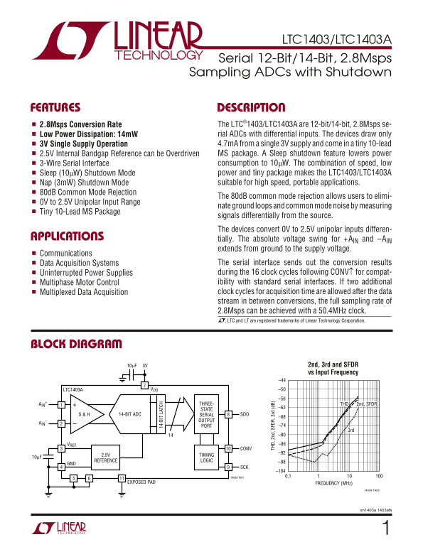
2.8Msps Conversion Rate The LTC®1403/LTC1403A are 12-bit/14-bit, 2.8Msps se- Low Power Dissipation: 14m W rial ADCs with differential inputs. The devices draw only 3V Single Supply Operation 4.7m A from a single 3V supply and come in a tiny 10-lead 2.5V Internal Bandgap Reference can be Overdriven MS package. A Sleep shutdown feature lowers power

-B IT AT CH

3-Wire Serial Interface consumption to 10µW. The combination of speed, low Sleep (10µW) Shutdown Mode power and tiny package makes the LTC1403/LTC1403A Nap (3m W) Shutdown Mode suitable for high speed, portable applications.

80d B Common Mode Rejection

The 80d B common mode rejection allows users to elimi-

0V to 2.5V Unipolar Input Range

nate ground loops and common mode noise by measuring

Tiny 10-Lead MS Package

signals differentially from the source. The devices convert 0V to 2.5V unipolar inputs differen-

APPLICATIO tially. The absolute voltage swing for +AIN and –AIN

extends from ground to the supply voltage.

Communications

Data Acquisition Systems The serial interface sends out the conversion results

Uninterrupted Power Supplies TH D, nd , S FD R, rd (d B) during the 16 clock cycles following CONV↑ for compat-

Multiphase Motor Control ibility with standard serial interfaces. If two additional Multiplexed Data Acquisition clock cycles for acquisition time are allowed after the data stream in between conversions, the full sampling rate of 2.8Msps can be achieved with a 50.4MHz clock. , LTC and LT are registered trademarks of Linear Technology Corporation.

BLOCK DIAGRA

3V10µF 2nd, 3rd and SFDR vs Input Frequency

LTC1403A VDD –50

AIN +1 THREE- THD 2nd, SFDR

STATE

S & H 14-BIT ADC SERIAL SDO

OUTPUT

PORT –74

–80 VREF –86

2.5V TIMING

REFERENCE LOGIC

–104 1403A TA015 0.1

EXPOSED PAD FREQUENCY (MHz)

1403A TA02

sn1403a 1403afs

Page Summary Contents For LINEAR TECHNOLOGY - 1 LTC1403 LTC1403A Data Sheet

Page 1 LTC1403/LTC1403A Serial 12-Bit/14-Bit, 2.8Msps Sampling ADCs with Shutdown FEATURES DESCRIPTIO 2.8Msps Conversion Rate The LTC®1403/LTC1403A are 12-bit/14-bit, 2.8Msps se- Low Power Dissipation: 14m W...
Page 2 LTC1403/LTC1403A ABSOLUTE AXI U RATI GS PACKAGE/ORDER I FOR ATIO (Notes 1, 2) Supply Voltage (VDD) 4V ORDER PART Analog Input Voltage NUMBER (Note 3) ....................................–0.3V to (VDD ...
Page 3 LTC1403/LTC1403A DY A IC ACCURACY The ● denotes the specifications which apply over the full operating temperature range, otherwise specifications are at TA = 25°C. VDD = 3V LTC1403 LTC1403A SYMBOL PA...
Page 4 LTC1403/LTC1403A POWER REQUIRE E TS The ● denotes the specifications which apply over the full operating temperature range, otherwise specifications are at TA = 25°C. (Note 17) SYMBOL PARAMETER CONDIT...
Page 5 AG NI TU DE (d B) EN OB (B IT S) SN (d B) LTC1403/LTC1403A TYPICAL PERFOR A CE CHARACTERISTICS TA = 25°C, VDD = 3V (LTC1403A) ENOBs and SINAD THD, 2nd and 3rd vs Input vs Input Frequency Frequency SFD...
Page 6 EF (V AM PL IT UD (d B) LTC1403/LTC1403A TA = 25°C, VDD = 3V (LTC1403A)TYPICAL PERFOR A CE CHARACTERISTICS Differential and Integral Linearity LI NE AR IT (L SB vs Conversion Rate SINAD vs Conversion ...
Page 7 LTC1403/LTC1403A PI FU CTIO S + (Pin 1): Noninverting Analog Input. AIN + operates AIN 10µF tantalum in parallel with 0.1µF ceramic). Keep in – with a 0V to 2.5V fully differentially with respect to A...
Page 8 LTC1403/LTC1403A UW TI I G DIAGRA LTC1403 Timing Diagram t6 t ACQ INTERNAL SAMPLE HOLD SAMPLE HOLD S/H STATUS SDO REPRESENTS THE ANALOG INPUT FROM THE PREVIOUS CONVERSION Hi-Z Hi-Z SDO D11 D10 D8 D7 D...
Page 9 LTC1403/LTC1403A APPLICATIO S I FOR ATIO DRIVING THE ANALOG INPUT detailed information is available in the Linear Technology Databooks and on the Linear View TM CD-ROM.) The differential analog inputs...
Page 10 LTC1403/LTC1403A APPLICATIO S I FOR ATIO 151Ω AIN 3VREF VREF AIN LTC1403/ LTC1403/ LTC1403A LTC1403A VREF Figure 1. RC Input Filter Figure 2 INPUT FILTERING AND SOURCE IMPEDANCE INPUT RANGE The noise ...
Page 11 LTC1403/LTC1403A CM RR (d B) APPLICATIO S I FOR ATIO LTC1403/LTC1403A Transfer Characteristic CMRR vs Frequency FS – 1LSB0 FREQUENCY (Hz) INPUT VOLTAGE (V) Figure 3 Figure 4 NI PO LA OU TP UT OD INPUT...
Page 12 LTC1403/LTC1403A APPLICATIO S I FOR ATIO optimum performance, a 10µF surface mount AVX capaci- tor with a 0.1µF ceramic is recommended for the VDD and VREF pins. Alternatively, 10µF ceramic chip capac...
Page 13 LTC1403/LTC1403A APPLICATIO S I FOR ATIO CONV, without any intervening rising edges at SCK, put sync input of the processor serial port. It is good practice the LTC1403/LTC1403A in Sleep mode and the ...
Page 14 LTC1403/LTC1403A APPLICATIO S I FOR ATIO LTC1403A first and then buffer this signal with the appro- HARDWARE INTERFACE TO TMS320C54x priate number of inverters to drive the serial clock input of The L...
Page 15 LTC1403/LTC1403A APPLICATIO S I FOR ATIO ; 01-08-01 ****************************************************************** ; Files: 014SI.ASM -> 1403A Sine wave collection with Serial Port interface ; ...
Page 16 LTC1403/LTC1403A ; -------------------dummy bsend return------------------------ bsend return_enable ;this is also a dummy return to define bsend ;in vector table file BVECTORS.ASM ; -----------------...
Page 17 LTC1403/LTC1403A * negative edge BCLKR * negative BFSR pulse * no data shifted * 1' cable from counter to CONV at DUT * 2' cable from counter to CLK at DUT *No right shift is needed to right justify t...
Page 18 LTC1403/LTC1403A APPLICATIO S I FOR ATIO ; All other vector locations are free to use. When programming always be sure ; the HPIINT bit is unmasked (IMR=200h) to allow the communications kernel and ; ...
Page 19 LTC1403/LTC1403A PACKAGE DESCRIPTIO MSE Package 10-Lead Plastic MSOP (Reference LTC DWG # 05-08-1663) BOTTOM VIEW OF EXPOSED PAD OPTION TYP BSC (NOTE 3) RECOMMENDED SOLDER PAD LAYOUT (NOTE 4) DETAIL “...
Page 20 LTC1403/LTC1403A RELATED PARTS PART NUMBER DESCRIPTION COMMENTS ADCs LTC1608 16-Bit, 500ksps Parallel ADC ±5V Supply, ±2.5V Span, 90d B SINAD LTC1604 16-Bit, 333ksps Parallel ADC ±5V Supply, ±2.5V Spa...

Manual Details

Brand Linear
Pages 20
File Size 270.74 KB
Published May 30, 2026
72 views

Enter the captcha to get the download link:

captcha

Frequently Asked Questions

What is the maximum data rate of this ADC?

It features a conversion rate of up to 2.8Msps.

Does it support different input voltages?

The device supports operation with unique unipolar inputs ranging from 0V to 2.5V.

How does the unit handle common noise in signals?

It offers 80dB Common Mode Rejection (CMRR) at 1MHz, minimizing ground loops and common mode noise.

What is the power consumption when idle or seldom used?

The Sleep shutdown feature reduces power consumption to 10mW, while Shutdown Mode draws only 3mW.