LINEAR LTC1983-3 LTC1983-5 Data Sheet User Manual
Summary
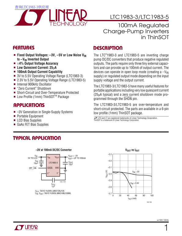
These highly efficient Inverting Charge Pump DC/DC converters (LTC1983 series) are designed for reliable generation of fixed negative voltages (-3V or -5V) from a single positive supply. Featuring up to 100mA output current and ultra-low quiescent draw, the unit is ideal for connecting low-power bias supplies in portable electronics and sophisticated systems like LCD biasing. The manual details its operation in both regulated and open-loop modes, ensuring protection against over-temperature and short circuits for demanding power applications.
Page 1 Text Content
查询LTC1983-3供应商
LTC1983-3/LTC1983-5 100m A Regulated Charge-Pump Inverters
in Thin SOT
FEATURES DESCRIPTIO Fixed Output Voltages: –3V, –5V or Low Noise VIN The LTC®1983-3 and LTC1983-5 are inverting charge to –VIN Inverted Output pump DC/DC converters that produce negative regulated ±4% Output Voltage Accuracy outputs. The parts require only three tiny external capaci- Low Quiesient Current: 25µA tors and can provide up to 100m A of output current. The 100m A Output Current Capability devices can operate in open loop mode (creating a –VIN 3V to 5.5V Operating Voltage Range (LTC1983-3) supply) or regulated output mode depending on the input 2.3V to 5.5V Operating Voltage Range (LTC1983-5) supply voltage and the output current. Internal 900k Hz Oscillator
The LTC1983-3/LTC1983-5 have many useful features for
“Zero Current” Shutdown
portable applications including very low quiescent current
Short-Circuit and Over-Temperature Protected
(25µA typical) and a zero current shutdown mode pro-
Low Profile (1mm) Thin SOTTM Package
grammed through the SHDN pin. APPLICATIO S The LTC1983-3/LTC1983-5 are over-temperature and
UT (V
short-circuit protected. The parts are available in a 6-pin
–3V Generation in Single-Supply Systems
low profile (1mm) Thin SOT package.■
Portable Equipment
, LTC and LT are registered trademarks of Linear Technology Corporation. LCD Bias Supplies Thin SOT is a trademark of Linear Technology Corporation.
Ga As FET Bias Supplies
TYPICAL APPLICATIO
–3V at 100m A DC/DC Converter VOUT vs IOUT
VIN VOUT = –3V
VIN VOUT
3V TO 5.5V IOUT = UP TO 100m A
CIN –3.2
10µF LTC1983-3
GND –3.1
OFF ON SHDN
VIN = 5V
1983-3 TA01
VIN = 3.3V
CFLY 1µF
CFLY: TAIYO YUDEN LMK212BJ105 CIN, COUT: TAIYO YUDEN JMK316BJ106ML –2.7
IOUT (m A)
1983 TA02
sn1983 1983fs
Page Summary Contents For LINEAR LTC1983-3 LTC1983-5 Data Sheet User Manual
Manual Details
| Brand | Linear |
|---|---|
| Pages | 12 |
| File Size | 176.74 KB |
| Published | June 16, 2026 |
Enter the captcha to get the download link:

Frequently Asked Questions
What negative voltages can this converter produce?
It is designed to generate fixed, regulated output voltages of either –3V or –5V.
How do I start using this device?
The parts require only three tiny external capacitors for proper operation.
Is this unit suitable for battery-powered equipment?
Yes; it features a zero current shutdown mode and very low quiescent current, ideal for portable applications.
What is the maximum output capacity of the converters?
The devices can provide up to 100mA of output current while maintaining stability.