LINEAR LTC1517-5 Data Sheet
Summary
This datasheet details the LTC1517-5, an ultralow power charge pump DC/DC converter that reliably generates a regulated 5V output for battery-powered electronics. Featuring low input current (typ. 6μA) and minimal external components, it is ideal for portable applications like cellular phones and handheld instruments requiring efficiency between 2.7V and 5V inputs. This manual provides detailed electrical characteristics, performance graphs on ripple and efficiency, and design guidelines essential for embedded system engineers customizing power supplies for small, advanced devices.
Page 1 Text Content
LTC1517-5
Micropower, Regulated 5V Charge Pump in a 5-Pin SOT-23 Package
FEATURES DESCRIPTION
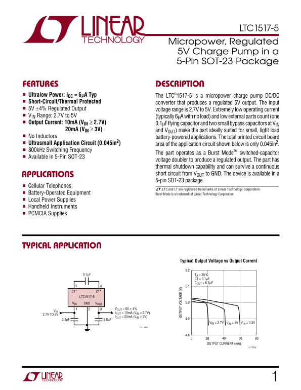
Ultralow Power: ICC = 6µA Typ The LTC®1517-5 is a micropower charge pump DC/DC Short-Circuit/Thermal Protected converter that produces a regulated 5V output. The input 5V ±4% Regulated Output voltage range is 2.7V to 5V. Extremely low operating current VIN Range: 2.7V to 5V (typically 6µA with no load) and low external parts count (one Output Current: 10m A (VIN ≥ 2.7V) 0.1µF flying capacitor and two small bypass capacitors at VIN
20m A (VIN ≥ 3V) and VOUT) make the part ideally suited for small, light load
No Inductors battery-powered applications. The total printed circuit board Ultrasmall Application Circuit (0.045in2) area of the application circuit shown below is only 0.045in2. 800k Hz Switching Frequency
The part operates as a Burst Mode TM switched-capacitor
Available in 5-Pin SOT-23
voltage doubler to produce a regulated output. The part has thermal shutdown capability and can survive a continuous APPLICATIONS short circuit from VOUT to GND. The device is available in a
OU TP UT OL TA GE (V 5-pin SOT-23 package.
Cellular Telephones
, LTC and LT are registered trademarks of Linear Technology Corporation.
Battery-Operated Equipment Burst Mode is a trademark of Linear Technology Corporation. Local Power Supplies Handheld Instruments PCMCIA Supplies
TYPICAL APPLICATION
Typical Output Voltage vs Output Current
0.1µF TA = 25°C
C1 = 0.1µF COUT = 6.8µF 5.1
LTC1517-5
VIN GND VOUT 5.0
VOUT = 5V ± 4%
IOUT = 10m A (VIN ≥ 2.7V)
2.7V TO 5V
IOUT = 20m A (VIN ≥ 3V)
VIN = 3.3VVIN = 3VVIN = 2.7V
1517 TA01
OUTPUT CURRENT (m A)
1517 TA02
Page Summary Contents For LINEAR LTC1517-5 Data Sheet
Manual Details
| Brand | Linear |
|---|---|
| Pages | 9 |
| File Size | 196.82 KB |
| Published | June 19, 2026 |
Enter the captcha to get the download link:

Frequently Asked Questions
What is the typical input current at no load?
Typically 6μA.
Does this device have protected features?
Yes, it features Short-Circuit/Thermal Protection and thermal shutdown capability.
What is the regulated output voltage range?
The output voltage range is between 2.7V and 5V.
How large is the application circuit area?
The total printed circuit board application circuit area is very small, only 0.045in.