LINEAR TECHNOLOGY LT3473 Micropower 1A Boost Converter with Schottky LINEAR TECHNOLOGY LT3473A Micropower 1A Boost Converter with Schottky and Output Disconnect
Summary
This highly integrated micropower boost converter provides robust DC/DC voltage boosting up to 34V in a miniature package. Engineered for maximum efficiency at light loads via automatic burst mode and featuring an internal Schottky diode, it is ideal for battery-powered, space-constrained electronics. The included manual delivers comprehensive technical specifications, electrical performance curves, and application details necessary for designing reliable, energy-efficient power management systems.
Page 1 Text Content
LT3473/LT3473A
Micropower 1A Boost POW ER LOSS (m
Converter with Schottky and Output Disconnect
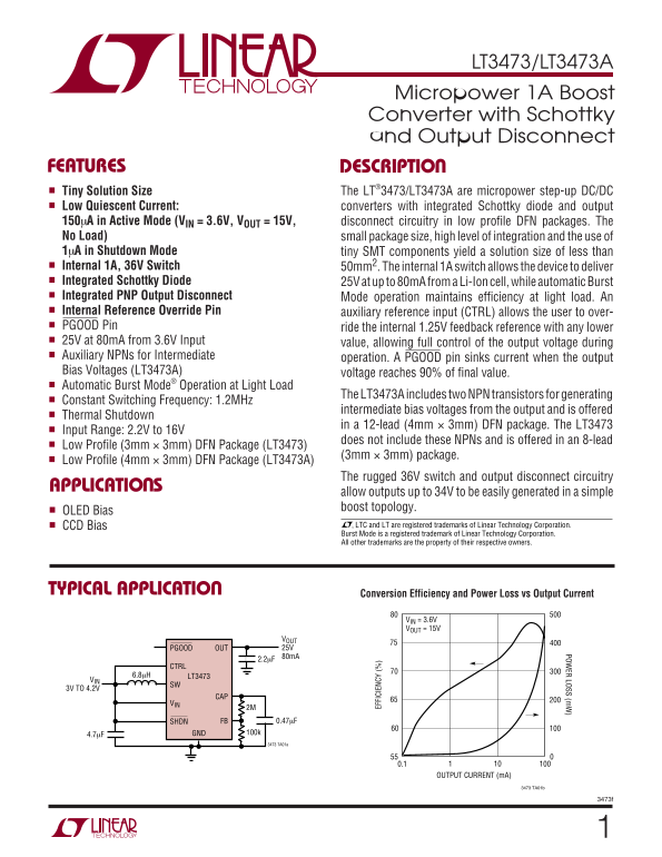
FEATURES DESCRIPTIO Tiny Solution Size The LT®3473/LT3473A are micropower step-up DC/DC Low Quiescent Current: converters with integrated Schottky diode and output 150µA in Active Mode (VIN = 3.6V, VOUT = 15V, disconnect circuitry in low profile DFN packages. The No Load) small package size, high level of integration and the use of 1µA in Shutdown Mode tiny SMT components yield a solution size of less than Internal 1A, 36V Switch 50mm2. The internal 1A switch allows the device to deliver Integrated Schottky Diode 25V at up to 80m A from a Li-Ion cell, while automatic Burst Integrated PNP Output Disconnect Mode operation maintains efficiency at light load. An Internal Reference Override Pin auxiliary reference input (CTRL) allows the user to over- PGOOD Pin ride the internal 1.25V feedback reference with any lower 25V at 80m A from 3.6V Input value, allowing full control of the output voltage during Auxiliary NPNs for Intermediate operation. A PGOOD pin sinks current when the output Bias Voltages (LT3473A) voltage reaches 90% of final value.
EF FI CI EN CY
Automatic Burst Mode® Operation at Light Load
The LT3473A includes two NPN transistors for generating
Constant Switching Frequency: 1.2MHz
intermediate bias voltages from the output and is offered
Thermal Shutdown
in a 12-lead (4mm × 3mm) DFN package. The LT3473
Input Range: 2.2V to 16V
does not include these NPNs and is offered in an 8-lead
Low Profile (3mm × 3mm) DFN Package (LT3473)
(3mm × 3mm) package.
Low Profile (4mm × 3mm) DFN Package (LT3473A)
The rugged 36V switch and output disconnect circuitry
APPLICATIO S
allow outputs up to 34V to be easily generated in a simple boost topology.
OLED Bias
CCD Bias , LTC and LT are registered trademarks of Linear Technology Corporation. Burst Mode is a registered trademark of Linear Technology Corporation. All other trademarks are the property of their respective owners.
TYPICAL APPLICATIO Conversion Efficiency and Power Loss vs Output Current
VIN = 3.6V VOUT = 15V
VOUT PGOOD OUT 25V 80m A 2.2µF
6.8µH LT3473
3V TO 4.2V
SHDN FB 0.47µF
4.7µF GND 100k 3473 TA01a
OUTPUT CURRENT (m A)
3473 TA01b
Page Summary Contents For LINEAR TECHNOLOGY LT3473 Micropower 1A Boost Converter with Schottky LINEAR TECHNOLOGY LT3473A Micropower 1A Boost Converter with Schottky and Output Disconnect
Manual Details
| Brand | Linear |
|---|---|
| Pages | 12 |
| File Size | 265.09 KB |
| Published | June 15, 2026 |
Enter the captcha to get the download link:

Frequently Asked Questions
What is the input voltage range of the LT3473?
The input voltage range is 2.2V to 16V.
What is the maximum output current at 25V from a 3.6V input?
It can deliver 25V at up to 80mA from a 3.6V input.
What package does the LT3473A use?
The LT3473A uses a 12-lead 4mm × 3mm DFN package.
What is the quiescent current in shutdown mode?
The quiescent current in shutdown mode is 1µA.