LINEAR TECHNOLOGY LT1017 LT1018 Micropower Dual Comparator User Guide
Summary
These micropower dual comparators are highly efficient components designed for designers of low-power, battery-operated monitoring systems. The LT1017 and LT1018 offer robust voltage comparison across a wide range (1.1V–40V), featuring extremely low power consumption and minimal offset voltage. This manual details the electrical specifications, applications, and pinouts for these high-performance comparators, making them ideal for continuous monitoring applications like alarms that require stable performance and current efficiency.
Page 1 Text Content
LT1017/LT1018 Micropower Dual Comparator
FEATURES DESCRIPTIO
Maximum Offset Voltage: 1m V The LT®1017/LT1018 are general purpose micropower Maximum Bias Current: 15n A comparators. The LT1017 is optimized for lowest operat- Typical Output Drive: 70m A ing power while the LT1018 operates at higher power and Operates from 1.1V to 40V higher speed. Both devices can operate from a single 1.1V Internal Pull-Up Current cell up to 40V. The output stage includes a class “B” pull- Output Can Drive Loads Above V+ up current source, eliminating the need for an external 30µA Supply Current (LT1017) resistive pull-up and saving power. The output stage is 110µA Supply Current (LT1018) also designed to allow driving loads connected to a supply more positive than the device, as can comparators with open-collector output stages.
APPLICATIO S
Input specifications are also excellent. On-chip trimming
Power Supply Monitors
minimizes offset voltage, while high gain and common
Relay Driving
SU PP LY UR RE NT (µ A) mode rejection ratio keep other input referred errors low.
Oscillators
Common mode voltage range includes ground. Special circuitry prevents false output states even if the input is overdriven. The LT1017/LT1018 are pin compatible with older dual comparators such as 393 type devices. , LTC and LT are registered trademarks of Linear Technology Corporation.
TYPICAL APPLICATIO
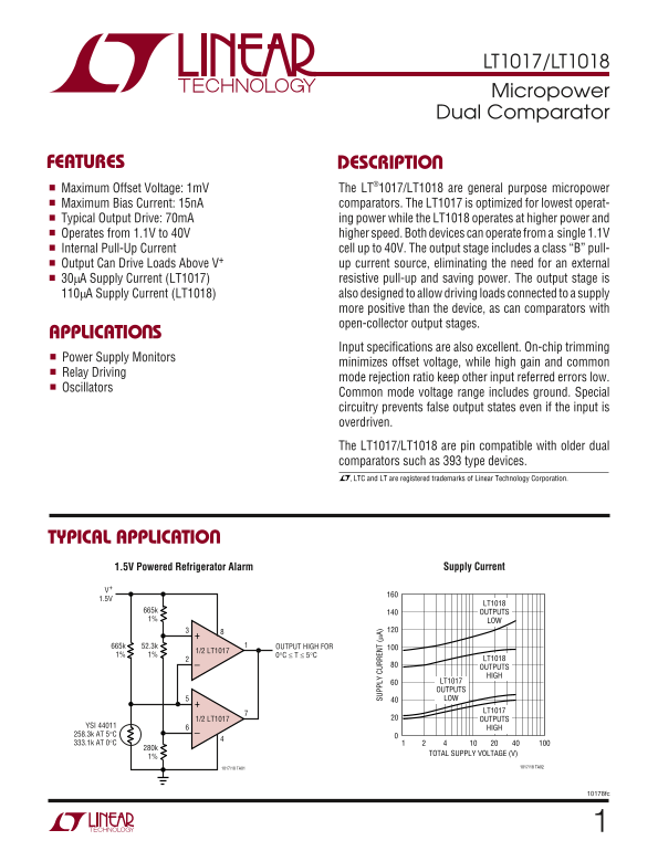
1.5V Powered Refrigerator Alarm Supply Current
LT1018
665k OUTPUTS 1% LOW
665k 52.3k OUTPUT HIGH FOR
1/2 LT1017
LT1018 OUTPUTS HIGH
LT1017 OUTPUTS LOW
LT1017
1/2 LT1017 OUTPUTS
YSI 44011
258.3k AT 5°C 333.1k AT 0°C
TOTAL SUPPLY VOLTAGE (V)
1017/18 TA01 1017/18 TA02
10178fc
Page Summary Contents For LINEAR TECHNOLOGY LT1017 LT1018 Micropower Dual Comparator User Guide
Manual Details
| Brand | Linear |
|---|---|
| Pages | 12 |
| File Size | 215.13 KB |
| Published | May 29, 2026 |
Enter the captcha to get the download link:

Frequently Asked Questions
What operating voltage range is supported by the LT1017/LT1018?
The comparators can operate from a single 1.1V up to 40V.
Which grade offers the highest temperature rating for operation?
M grade parts support temperatures ranging from –55°C to 125°C.
Does the output stage require an external pull-up resistor?
No, the internal class 'B' pull-up current source eliminates the need for an external resistive pull-up.
How does the LT1017 compare to the LT1018 in performance?
The LT1017 is optimized for lowest power while the LT1018 operates at higher power and higher speed.
What is the typical maximum offset voltage for these comparators?
The typical max offset voltage across various temperature ranges generally remains low, around 0.4–1mV at room temperature.