# A B C D E F G H I J K L M N O P Q R S T U V W X Y Z

LINEAR TECHNOLOGY LTC1735 User Guide

Summary

The LTC1735 is a high-efficiency synchronous step-down switching regulator designed for advanced DC power management systems. This manual provides comprehensive technical documentation, covering electrical characteristics across wide operating ranges (4V to 36V), including optimized features like OPTI-LOOP compensation and Burst Mode operation. It details the setup, advanced protection features (e.g., Undervoltage/Overvoltage Crowbar), and precise application usage. This documentation is essential for hardware engineers and power electronics designers building reliable, high-performance embedded systems such as notebooks, PDAs, and industrial power distribution networks.
📄 Preview PAGE OF 32

Page 1 Text Content

LTC1735 High Efficiency

Synchronous Step-Down Switching Regulator

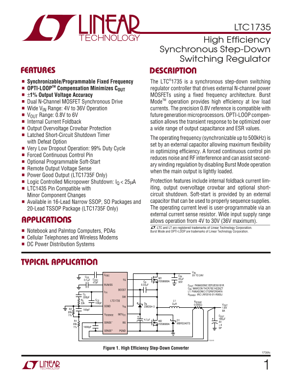
FEATURES DESCRIPTIO Synchronizable/Programmable Fixed Frequency The LTC®1735 is a synchronous step-down switching OPTI-LOOPTM Compensation Minimizes COUT regulator controller that drives external N-channel power ±1% Output Voltage Accuracy MOSFETs using a fixed frequency architecture. Burst Dual N-Channel MOSFET Synchronous Drive Mode TM operation provides high efficiency at low load Wide VIN Range: 4V to 36V Operation currents. The precision 0.8V reference is compatible with VOUT Range: 0.8V to 6V future generation microprocessors. OPTI-LOOP compen- Internal Current Foldback sation allows the transient response to be optimized over Output Overvoltage Crowbar Protection a wide range of output capacitance and ESR values. Latched Short-Circuit Shutdown Timer

The operating frequency (synchronizable up to 500k Hz) is

with Defeat Option

set by an external capacitor allowing maximum flexibility

Very Low Dropout Operation: 99% Duty Cycle

in optimizing efficiency. A forced continuous control pin

Forced Continuous Control Pin

reduces noise and RF interference and can assist second-

Optional Programmable Soft-Start

ary winding regulation by disabling Burst Mode operation

Remote Output Voltage Sense

when the main output is lightly loaded.

Power Good Output (LTC1735F Only)

Logic Controlled Micropower Shutdown: IQ < 25µA Protection features include internal foldback current lim- LTC1435 Pin Compatible with iting, output overvoltage crowbar and optional short- Minor Component Changes circuit shutdown. Soft-start is provided by an external Available in 16-Lead Narrow SSOP, SO Packages and capacitor that can be used to properly sequence supplies. 20-Lead TSSOP Package (LTC1735F Only) The operating current level is user-programmable via an external current sense resistor. Wide input supply range

APPLICATIO S allows operation from 4V to 30V (36V maximum).

, LTC and LT are registered trademarks of Linear Technology Corporation. Notebook and Palmtop Computers, PDAs Burst Mode and OPTI-LOOP are trademarks of Linear Technology Corporation.■

Cellular Telephones and Wireless Modems DC Power Distribution Systems

TYPICAL APPLICATIO

COSC CIN 5V TO 24V

0.1µF COSC TG

CB FDS6680A 50V

RUN/SS 0.22µF COUT: PANASONIC EEFUEOG181R

CIN: MARCON THCR70E1H226ZT

BOOST

ITH L1: PANASONIC ETQP6F2R0HFA

CC RSENSE: IRC LRF2010-01-R005J

330p F SW

RC CC2 LTC1735 L1

RSENSE

33k 100p F DB 2µH

0.005Ω VOUT

SGND VIN CMDSH-3

1% VOSENSE INTVCC

COUT 4.7µF 180µF

SENSE– BG 4V

20k FDS6680A MBRS340T3

SENSE+ PGND

Figure 1. High Efficiency Step-Down Converter

1735fc

Page Summary Contents For LINEAR TECHNOLOGY LTC1735 User Guide

Page 1 LTC1735 High Efficiency Synchronous Step-Down Switching Regulator FEATURES DESCRIPTIO Synchronizable/Programmable Fixed Frequency The LTC®1735 is a synchronous step-down switching OPTI-LOOPTM Compensa...
Page 2 LTC1735 ABSOLUTE AXI RATI GS (Note 1) Input Supply Voltage (VIN) .........................36V to –0.3V Peak Driver Output Current &lt;10µs (TG, BG) 3A Topside Driver Supply Voltage (BOOST)....42V to –...
Page 3 LTC1735 ELECTRICAL CHARACTERISTICS The ● denotes specifications which apply over the full operating temperature range, otherwise specifications are at TA = 25°C. VIN = 15V, VRUN/SS = 5V unless otherwi...
Page 4 EF FI CI EN CY EF FI CI EN CY LTC1735 ELECTRICAL CHARACTERISTICS Note 3: The LTC1735 is tested in a feedback loop that servos VOSENSE to Note 6: The minimum on-time condition corresponds to an inducto...
Page 5 AX IM UM UR RE NT EN SE HR ES HO LD (m V) AX IM UM UR RE NT EN SE HR ES HO LD (m V) IN PU CU RR EN (µ A) LTC1735 TYPICAL PERFOR A CE CHARACTERISTICS Input and Shutdown Currents EXTVCC Switch Drop vs I...
Page 6 FR EQ UE NC (k Hz EN SE (µ A) LTC1735 TYPICAL PERFOR A CE CHARACTERISTICS SU PP LY UR RE NT (µ A) ITH Voltage vs Load Current Output Current vs Duty Cycle SENSE Pins Total Source Current 2.5 VIN = 10V...
Page 7 LTC1735 TYPICAL PERFOR A CE CHARACTERISTICS VOUT(RIPPLE) (Burst Mode Operation) Load Step (Burst Mode Operation) Load Step (Continuous Mode) FIGURE 1 FIGURE 1 FIGURE 1ILOAD = 1.5A VOUT VOUT 20m V/DIV ...
Page 8 LTC1735 PI FU CTIO VOSENSE: Receives the feedback voltage from an external INTVCC: Output of the Internal 5.2V Regulator and EXTVCC resistive divider across the output. Switch. The driver and control ...
Page 9 LTC1735 FU CTIO AL DIAGRA 0.8V UVL PGOOD INTVCC 0.17µA FCBSGNDCOSC FC DB BOOST SYNC OSC VSEC FORCE BOT DROP OUT SW LTC1735F CSEC DET BOT ONLY SWITCH LOGIC TOP ON D1 2.4V SD 2k 45k 45k VOUT VOSENSE VFB...
Page 10 LTC1735 OPERATIO (Refer to Functional Diagram) The main control loop is shut down by pulling Pin 2 When the FCB pin is driven by an external oscillator, a low (RUN/SS) low. Releasing RUN/SS allows an ...
Page 11 LTC1735 OPERATIO (Refer to Functional Diagram) INTVCC/EXTVCC POWER To provide clean start-up and to protect the MOSFETs, undervoltage lockout is used to keep both MOSFETs off Power for the top and bot...
Page 12 LTC1735 SC AL UE (p F) APPLICATIO S I FOR ATIO The internal oscillator runs at its nominal frequency (f O) of smaller inductor and capacitor values. So why would when the FCB pin is pulled high to INT...
Page 13 LTC1735 APPLICATIO S I FOR ATIO Ferrite designs have very low core loss and are preferred The MOSFET power dissipations at maximum output at high switching frequencies, so design goals can con- curren...
Page 14 LTC1735 APPLICATIO S I FOR ATIO CIN Selection The first condition relates to the ripple current into the ESR of the output capacitance while the second term guaran- In continuous mode, the source curr...
Page 15 LTC1735 APPLICATIO S I FOR ATIO capacitor available from Sanyo has the lowest (ESR)(size) within the LTC1735. The INTVCC pin can supply a maxi- product of any aluminum electrolytic at a somewhat mum R...
Page 16 LTC1735 APPLICATIO S I FOR ATIO derived from the output or other external source during Output Voltage Programming normal operation. When the output is out of regulation The output voltage is set by a...
Page 17 LTC1735 APPLICATIO S I FOR ATIO VOUT resistive divider. The maximum current flowing out R2 of the sense pins is: VOSENSE + + ISENSE – = (2.4V – VOUT)/24k ISENSE LTC1735 R147p F SGND Since VOSENSE is s...
Page 18 LTC1735 APPLICATIO S I FOR ATIO Diode D1 in Figure 5 reduces the start delay while allowing capacitor during a severe overcurrent and/or short-circuit CSS to charge up slowly for the soft-start functi...
Page 19 LTC1735 APPLICATIO S I FOR ATIO t ON(MIN) of the LTC1735 (approximately 200ns), the input the gate charge required to turn on the top MOSFET. Low voltage and inductor value: duty cycle applications ma...
Page 20 LTC1735 APPLICATIO S I FOR ATIO FCB Pin Operation include this current when choosing resistor values R3 and R4. When the FCB pin drops below its 0.8V threshold, continu- ous mode operation is forced. ...
Page 21 LTC1735 APPLICATIO S I FOR ATIO Although all dissipative elements in the circuit produce 4) Transition losses apply only to the topside MOSFET(s) losses, 4 main sources usually account for most of the...
Page 22 LTC1735 APPLICATIO S I FOR ATIO The ITH series RC–CC filter sets the dominant pole-zero Active voltage positioning improves transient response loop compensation. The values can be modified slightly an...
Page 23 LTC1735 APPLICATIO S I FOR ATIO R3 680k VIN 7.5V TO R1 R4 C7 C12 TO C14 24V 27k 100k 0.1µF 10µF 35V C9, C19: TAIYO YUDEN JMK107BJ105 C1 GND C10: KEMET T494A475M010AS C12 TO C14: TAIYO YUDEN GMK325F106...
Page 24 LTC1735 APPLICATIO S I FOR ATIO At full load current: The Thevenin equivalent of the gain limiting resistance value of 17.54k is made up of a resistor R4 that sources current into the ITH pin and resi...
Page 25 LTC1735 APPLICATIO S I FOR ATIO The network shown in Figure␣ 11 is the most straight VIN = 12V FIGURE 8 CIRCUIT VOUT = 1.5V OUTPUT forward approach to protect a DC/DC converter from the VOLTAGE ravage...
Page 26 LTC1735 APPLICATIO S I FOR ATIO Next verify the minimum on-time of 200ns is not violated. CIN is chosen for an RMS current rating of at least 2.5A at The minimum on-time occurs at maximum VIN: tempera...
Page 27 LTC1735 APPLICATIO S I FOR ATIO the INTVCC and PGND pins can help improve noise feedback pins. All of these nodes have very large and fast performance. moving signals and therefore should be kept on t...
Page 28 LTC1735 TYPICAL APPLICATIO 1.8V/5A Converter from Design Example with Burst Mode Operation Disabled VIN 4.5V TO 22V COSC CIN 43p F 22µF 50V COSC TG CER CSS CB Si4412DY RUN/SS BOOST CC 470p FRC 33k ITH...
Page 29 LTC1735 TYPICAL APPLICATIO Selectable Output Voltage Converter with Burst Mode Operation Disabled for CPU Power VIN 0.1µF 4.5V TO 24V NC NC NCNC CIN COSC TG CER CSS CB FDS6680A CIN: MARCON THCR70EIH22...
Page 30 LTC1735 TYPICAL APPLICATIO 5V/3.5A Converter with 12V/200m A Auxiliary Output VIN 5.5V TO 28V COSC CIN 51p F 22µF M1 30V COSC TG OS-CON CSS CB Si4802DY RUN/SS BOOST CC MBRS1100T3 470p FRC 33k ITH SW C...
Page 31 LTC1735 PACKAGE DESCRIPTION F Package 20-Lead Plastic TSSOP (4.4mm) (Reference LTC DWG # 05-08-1650) (.018 – .030) BSC 4.50 ±0.106.60 ±0.10 (.0036 – .0079) BSC (.002 – .006) 0.195 – 0.30 (.0077 – .011...
Page 32 LTC1735 TYPICAL APPLICATIO 3.3V to 2.5V/5A Converter with External Clock Synchronization Operating at 500k Hz VIN 0.1µF 3.3V5V COSC CIN 20p F 100µF M1 10V COSC TG OS-CON CSS CB Si4410DY RUN/SS BOOST C...

Manual Details

Brand Linear
Pages 32
File Size 401.47 KB
Published May 25, 2026
187 views

Enter the captcha to get the download link:

captcha

Frequently Asked Questions

What input voltage range does the LTC1735 support?

It operates from a wide input supply range, allowing operation from 4V to 36V (maximum).

How can I adjust the switching frequency?

The operating frequency is synchronizable up to 500kHz. This frequency is set by an external capacitor.

Does it have protection against output overvoltage?

Yes, it features Output Overvoltage Crowbar Protection and internal foldback current limiting for protection.

Which function optimizes efficiency at low loads?

The Burst Mode dual N-channel MOSFET synchronous drive mode provides high efficiency specifically at low load conditions.