LINEAR TECHNOLOGY LT3464 User Guide
Summary
This micropower boost converter (LT3464) is engineered to provide highly efficient, compact power solutions for battery-powered devices like handheld computers and LCD displays. Featuring a minuscule footprint and extremely low quiescent current (<0.5µA), it integrates key components such as an output disconnect and Schottky diode, enabling robust power management up to 16V from varied inputs. The manual provides comprehensive details on electrical characteristics, operating limits, and performance parameters necessary for system designers creating miniature, high-reliability circuits.
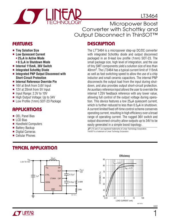
Page 1 Text Content
LT3464
Micropower Boost
Converter with Schottky and Output Disconnect in Thin SOT™ FEATURES DESCRIPTIO
Tiny Solution Size The LT®3464 is a micropower step-up DC/DC converter Low Quiescent Current with integrated Schottky diode and output disconnect • 25µA in Active Mode packaged in an 8-lead low profile (1mm) SOT-23. The
• 0.5µA in Shutdown Mode small package size, high level of integration, and the use Internal 115m A, 36V Switch of tiny SMT components yield a solution size of less than Integrated Schottky Diode 40mm2. The LT3464 has a typical current limit of 115m A
Integrated PNP Output Disconnect with as well as fast switching speed to allow the use of a chip Short-Circuit Protection inductor and small ceramic capacitors. The internal PNP Internal Reference Override Pin disconnects the output load from the input during shut- 16V at 8m A from 3.6V Input down, and also provides output short-circuit protection. 12V at 20m A from 5V Input An auxiliary reference input allows the user to override the Input Range: 2.3V to 10V internal 1.25V feedback reference with any lower value, High Output Voltage: Up to 34V allowing full control of the output voltage during opera-
EF FI CI EN CY
Low Profile (1mm) SOT-23 Package tion. This device features a low 25µA quiescent current,
which is further reduced to less than 0.5µA in shutdown. APPLICATIO A current limited fixed off-time control scheme conserves operating current, resulting in high efficiency over a broad
OEL Panel Bias
range of operating current. The rugged 36V switch and
LCD Bias
output disconnect circuitry allow outputs up to 34V to be
Handheld Computers
easily generated in a simple boost topology.
Battery Backup
, LTC and LT are registered trademarks of Linear Technology Corporation. Digital Cameras Thin SOT is a trademark of Linear Technolgy Corporation
Cellular Phones
TYPICAL APPLICATIO
Efficiency
VIN 2.3V TO 10V
VIN = 8.4V
VIN SW
VIN = 4.2V
CTRL 0.22µF
LT3464 CAP
SHDN 0.33µF 3.48M
FB GND 294k
3464 TA01a
0.01 0.1 LOAD CURRENT (m A)
3634 TA01b
Page Summary Contents For LINEAR TECHNOLOGY LT3464 User Guide
Manual Details
| Brand | Linear |
|---|---|
| Pages | 16 |
| File Size | 236.00 KB |
| Published | June 06, 2026 |
Enter the captcha to get the download link:

Frequently Asked Questions
What is the low power consumption of this DC/DC converter?
It has a quiescent current of 25μA in Active Mode, which reduces to less than 0.5μA in Shutdown Mode.
What is the maximum output voltage supported by the LT3464?
The device supports a high output voltage, reaching up to 34V.
Does the unit offer protection against electrical faults?
Yes, it includes an internal PNP output disconnect and provides built-in output short-circuit protection.
What is the acceptable input voltage range for operation?
The LT3464 can operate safely with an input voltage ranging from 2.3V to 10V.