# A B C D E F G H I J K L M N O P Q R S T U V W X Y Z

LINEAR TECHNOLOGY LTC3713 User Guide

Summary

This manual provides detailed technical specifications for the LTC3713, a high-efficiency synchronous buck switching regulator controller. The product is engineered for low-voltage power systems, featuring operation from as low as 1.5V and eliminating the need for external sense resistors. It includes advanced protections like programmable soft-start and overvoltage monitoring. This resource is essential for electrical engineers designing compact, reliable power management solutions, particularly in demanding applications such as telecommunications equipment that require stable step-down voltage regulation.
📄 Preview PAGE OF 24

Page 1 Text Content

LTC3713

Low Input Voltage,

High Power, No RSENSE

Synchronous Buck DC/DC Controller

FEATURES DESCRIPTIO

Very Low VIN(MIN): 1.5V The LTC®3713 is a high current, high efficiency synchro- True Current Mode Control nous buck switching regulator controller optimized for 5V Drive for N-Channel MOSFETs Eliminates use with very low input supply voltages. It operates from Auxillary 5V Supply inputs as low as 1.5V and provides a regulated output No Sense Resistor Required voltage from 0.8V up to (0.9)VIN. The controller uses Uses Standard 5V Logic-Level N-Channel MOSFETs a valley current control architecture to enable high operat- Adjustable Current Limit ing frequencies without requiring a sense resistor. Adjustable Frequency Operating frequency is selected by an external resistor and Switch t ON(MIN) < 100ns is compensated for variations in VIN and VOUT. The LTC3713 2% to 90% Duty Cycle at 200k Hz uses a pair of standard 5V logic-level N-channel external 0.8V ±1% Reference MOSFETs, eliminating the need for expensive P-channel Power Good Output Voltage Monitor or low threshold devices.

Programmable Soft-Start

Discontinuous mode operation provides high efficiency

Output Overvoltage Protection

operation at light loads. A forced continuous control

Optional Short-Circuit Shutdown Timer

pin reduces noise and RF interference, and can assist

Small 24-Lead SSOP Package

secondary winding regulation by disabling discontinuous

EF FI CI EN CY operation when the main output is lightly loaded. Fault

APPLICATIO S

protection is provided by internal foldback current limit- Telecom Card 3.3V, 2.5V, 1.8V Step-Down ing, an output overvoltage comparator and an optional Bus Termination (DDR memory, SSTL) short-circuit shutdown timer.

Synchronous Buck with General Purpose Boost

, LTC and LT are registered trademarks of Linear Technology Corporation. Low VIN Synchronous Boost No RSENSE is a trademark of Linear Technology Corporation.

TYPICAL APPLICATIO

VIN 1.8V TO 3.3V

CMDSH-3

22µF SHDN BOOST ×2 Efficiency vs Load Current

5.6k VIN = 2.5V

ION TG M1 L1

LTC3713 1.8µH VOUT

VFB1 SW1 1.25V COUT 10A

SENSE+

680p F BG M2 ×2

ITH PGND

SENSE–

RUN/SS INTVCC

0.1µF PGOOD VIN1

SGND VIN2

COUT: PANASONIC EEFUEOD271R 4.7µHMBR0520 0.01

L1: (A) PANASONIC ETQP6FIR8BFA 0.04 0.10 0.40

(B) TOKO D104C-1.8µH LOAD CURRENT (A)

VFB2 SW2 M1, M2: (A) IRF7822, (B) IRF7811A

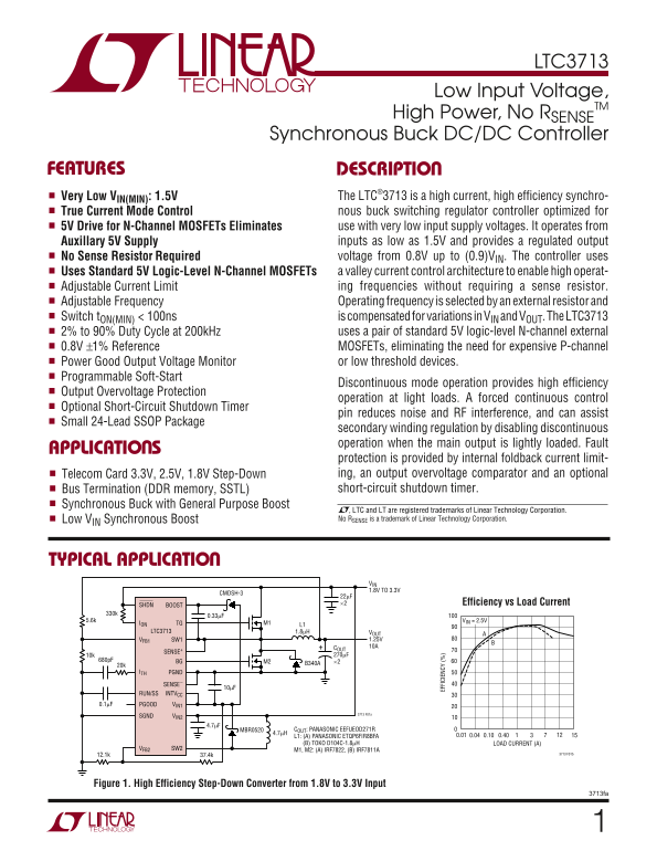
Figure 1. High Efficiency Step-Down Converter from 1.8V to 3.3V Input

3713fa

Page Summary Contents For LINEAR TECHNOLOGY LTC3713 User Guide

Page 1 LTC3713 Low Input Voltage, High Power, No RSENSE Synchronous Buck DC/DC Controller FEATURES DESCRIPTIO Very Low VIN(MIN): 1.5V The LTC®3713 is a high current, high efficiency synchro- True Current Mod...
Page 2 LTC3713 ABSOLUTE AXI U RATI GS PACKAGE/ORDER I FOR ATIO (Note 1) Input Supply Voltage (VIN2) .......................10V to –0.3V TOP VIEW ORDER PART Boosted Topside Driver Supply Voltage NUMBER RUN/SS...
Page 3 LTC3713 ELECTRICAL CHARACTERISTICS The ● denotes specifications which apply over the full operating temperature range, otherwise specifications are TA = 25°C. VIN1 = 15V, VIN2 = 1.5V unless otherwise ...
Page 4 SW IT CH IN FR EQ UE NC (M Hz FE ED BA CK IN OL TA GE (V LTC3713 TYPICAL PERFOR A CE CHARACTERISTICS Transient Response (Discontinuous Mode)Transient Response Start-Up from Shutdown VOUT VOUT 100m V/D...
Page 5 AX IM UM UR RE NT EN SE HR ES HO LD (m V) ON -T IM (n s) ∆V OU LTC3713 TYPICAL PERFOR A CE CHARACTERISTICS Frequency vs Input Voltage Load Regulation On-Time vs ION Current 10k VVON = 0V LOAD = 6A LOA...
Page 6 CU RR EN SE NS TH RE SH OL (m V) FE ED BA CK EF ER EN CE OL TA GE (V LTC3713 TYPICAL PERFOR A CE CHARACTERISTICS RU N/ SS HR ES HO LD (V Feedback Reference Voltage vs Error Amplifier gm vs INTVCC Load...
Page 7 LTC3713 PI FU CTIO S RUN/SS (Pin 1): Run Control and Soft-Start Input. A VFB2 (Pin 12): Boost Converter Feedback. The VFB2 pin is capacitor to ground at this pin sets the ramp time to full connected t...
Page 8 LTC3713 FU CTIO AL DIAGRA S VON VIN ION FCB VIN1 0.8V REF 5V REG BOOST VVON t ON = (10p F) CB IION TG FCNT M1 SENSE+ L1 SWITCH ICMP IREV DB VOUT LOGIC INTVCC 1.4V CVCC COUT PGND1 SENSE– PGOOD Q2 Q4 UV...
Page 9 LTC3713 OPERATIO Main Control Loop and M2 is turned on and held on until the overvoltage condition clears. The LTC3713 is a current mode controller for DC/DC step-down converters designed to operate f...
Page 10 LTC3713 OPERATIO switch cycle, turning on the switch. When the summation response can be optimized by the addition of a phase lead of a signal representing switch current and a ramp gen- capacitor CPL...
Page 11 LTC3713 APPLICATIO S I FOR ATIO SENSE+ The gate drive voltage is set by the 5V INTVCC supply. WITHOUT RSENSE Consequently, logic-level threshold MOSFETs must be used in LTC3713 applications. SENSE+ Wh...
Page 12 LTC3713 APPLICATIO S I FOR ATIO The resulting power dissipation in the MOSFETs at maxi- Hz OUT mum output current are: VON ON 2 ρT(TOP) RDS(ON)(MAX) PTOP = DTOP IOUT(MAX) To hold frequency constant du...
Page 13 LTC3713 APPLICATIO S I FOR ATIO specific application. A good starting point is to feed about of the bottom MOSFET from turning on and storing charge 25% of the voltage change at the ITH pin to the VON...
Page 14 LTC3713 APPLICATIO S I FOR ATIO Tantalum capacitors have the highest capacitance density Fault Conditions: Current Limit and Foldback but it is important to only use types that have been surge The max...
Page 15 LTC3713 APPLICATIO S I FOR ATIO due to a dropping input voltage for example, then the SS µ( )1 CDELAY SS= output will drop out of regulation. The minimum input voltage to avoid dropout is: When the vo...
Page 16 LTC3713 APPLICATIO S I FOR ATIO be estimated from: converter. To ensure that the ripple current doesn’t exceed a specified amount, the inductance can be chosen accord- CSS &gt; COUT • VOUT • RSENSE (1...
Page 17 LTC3713 APPLICATIO S I FOR ATIO loss. For example, if RDS(ON) = 0.01Ω and RL = 0.005Ω, the Design Example loss will range from 1% up to 10% as the output current As a design example, take a supply wit...
Page 18 LTC3713 APPLICATIO S I FOR ATIO However, a 0A to 6A load step will cause an output change of up to: ∆VOUT(STEP) = ∆ILOAD (ESR) = (6A) (0.005Ω) = 30m V p F k Hz The inductor for the boost converter is ...
Page 19 LTC3713 APPLICATIO S I FOR ATIO PC Board Layout Checklist Flood all unused areas on all layers with copper. Flooding with copper will reduce the temperature rise When laying out a PC board follow one ...
Page 20 LTC3713 TYPICAL APPLICATIO S 1.25V/±6A Bus Terminator RPG DB 100k CMDSH-3 VIN RUN/SS BOOST 2.5V CB TO 3.3V M1 B340A CIN1B VON TG IRF7811A 330µF CIN1A 22µF PGOOD PGOOD SW1 X5R 6.3V VRNG SENSE+ L1 ×2 VO...
Page 21 LTC3713 TYPICAL APPLICATIO S One-Half VIN/±6A Bus Terminator VIN CINA 1.8V TO 3.3V CINB CMDSH-3 RPG RUN/SS BOOST VON TG IRF7811A PGOOD PGOOD SW1 VRNG SENSE+ R1 R3 1µH VOUT 10k 5k 0.9V TO 1.65V D3 FCB ...
Page 22 LTC3713 TYPICAL APPLICATIO S Dual Output 1.25V/10A Buck Converter and 5V to 12V/130m A Boost Converter CSS RF DB 0.1µF 1Ω CMDSH-3 RUN/SS BOOST CB CINIA 5V TO 24V VON TG X5R IRF7811A PGOOD PGOOD SW1 VR...
Page 23 LTC3713 PACKAGE DESCRIPTIO G Package 24-Lead Plastic SSOP (5.3mm) (Reference LTC DWG # 05-08-1640) 0.42 ±0.03 0.65 BSC RECOMMENDED SOLDER PAD LAYOUT BSC 0.05 NOTE: (.002) G24 SSOP 0802 1. CONTROLLING ...
Page 24 LTC3713 TYPICAL APPLICATIO 3.3V to 5V Synchronous Boost Converter RPG DB L1 100k CMDSH-3 1.8µH RUN/SS BOOST CB 3.3V 0.33µF CINIA CINIB VON TG 22µF PGOOD PGOOD SW1 IRF7811A VOUT VRNG SENSE+ 5V 52.5k D1...

Manual Details

Brand Linear
Pages 24
File Size 280.49 KB
Published June 01, 2026
72 views

Enter the captcha to get the download link:

captcha

Frequently Asked Questions

What low voltage input levels can the LTC3713 operate from?

It operates with auxiliary supplies as low as 1.5V, even when needing to power N-Channel MOSFETs.

Does using an external sense resistor eliminate the need for a sense resistor?

No, the controller is designed to operate without requiring an external sense resistor (No R).

How can I adjust the operating frequency of the device?

The operating frequency is selected and controlled by integrating an external resistor into the circuit design.

What protective features does this DC/DC controller include?

It offers internal fault protection, including foldback current limit, output overvoltage protection, and short-circuit shutdown.