# A B C D E F G H I J K L M N O P Q R S T U V W X Y Z

LINEAR TECHNOLOGY LT1533 User Guide

Summary

Achieve exceptional electrical performance with this ultralow noise switching regulator designed for demanding environments. This precision component significantly minimizes conducted and radiated EMI, making it ideal for sensitive systems. The comprehensive manual covers rigorous electrical characteristics, operational parameters, and diverse circuit schematics. It is essential reading for engineers developing critical applications such as medical devices, industrial automation gear, wireless communication equipment, and single-board data acquisition systems requiring stable power and ultra-low noise.
📄 Preview PAGE OF 20

Page 1 Text Content

LT1533

Ultralow Noise

1A Switching Regulator FEATURES DESCRIPTION

Greatly Reduced Conducted and Radiated EMI The LT®1533 is a new class of switching regulator designed (<100µVP-P in Typical Application) to reduce conducted and radiated electromagnetic interfer- Low Switching Harmonic Content ence (EMI). Ultralow noise and EMI are achieved by providing Independent Control of Switch Voltage and user control of the output switch slew rates. Voltage and Current Slew Rates current slew rates can be independently programmed to Two 1A Current Limited Power Switches optimize switcher harmonic content versus efficiency. The Regulates Positive and Negative Voltages LT1533 can reduce high frequency harmonic power by as 20k Hz to 250k Hz Oscillator Frequency much as 40d B with only minor losses in efficiency. Easily Synchronized to External Clock

The LT1533 utilizes a dual output switch current mode

Wide Input Voltage Range: 2.7V to 23V

architecture optimized for low noise topologies. The IC

Low Shutdown Current: 12µA Typical

includes two 1A power switches along with all necessary

Easier Layout than with Conventional Switchers

oscillator, control and protection circuitry. Unique error amp

Outputs Can Be Forced to 50% Duty Cycle for

circuitry can regulate both positive and negative voltages.

Unregulated Applications

The internal oscillator may be synchronized to an external clock for more accurate placement of switching harmonics.

APPLICATIONS

Protection features include cycle by cycle current limit pro- tection, undervoltage lockout and thermal shutdown.

Precision Instrumentation Systems

Isolated Supplies for Industrial Automation Low minimum supply voltage and low supply current during

Medical Instruments shutdown make the LT1533 well suited for portable applica- Wireless Communications tions. The part may also be forced into a 50% duty cycle mode Single Board Data Acquisition Systems for unregulated applications. The LT1533 is available in the

16-pin narrow SO package.

, LTC and LT are registered trademarks of Linear Technology Corporation.

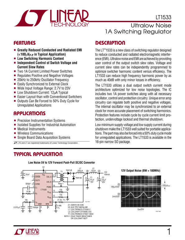
TYPICAL APPLICATION Low Noise 5V to 12V Forward Push-Pull DC/DC Converter

1N4148 300µH 33µH 12V Output Noise (BW = 100MHz) T1

33µF VIN 150m A

SHDN COL A

COL B 16V 20V

820p F SYNC Note 1

<100µVP-P

PGND 100µV/DIV

CT LT1533 15k

16.9k RVSL

RCSL 2m V/DIV

1533 TA01

VC FB

GND NFB

C1: SANYO OS-CON

0.015µF 1000p F C2: AVX TPS TANTALUM

L1: COILTRONICS CTX300-2 2µs/DIV

L2: COILCRAFT DT1608C-333 1533 TA02

T1: COILTRONICS CTX02-13834 NOTE 1: 25n H TRACE INDUCTANCE OR COILCRAFT B07T

Page Summary Contents For LINEAR TECHNOLOGY LT1533 User Guide

Page 1 LT1533 Ultralow Noise 1A Switching Regulator FEATURES DESCRIPTION Greatly Reduced Conducted and Radiated EMI The LT®1533 is a new class of switching regulator designed (&lt;100µVP-P in Typical Applica...
Page 2 LT1533 ABSOLUTE MAXIMUM RATINGS PACKAGE/ORDER INFORMATION (Note 1) Input Voltage (VIN) 30V TOP VIEW ORDER PART NUMBER Switch Voltage (COL A, COL B) 30V NC PGND SHDN Pin Voltage 30V COL A COL B Feedbac...
Page 3 LT1533 ELECTRICAL CHARACTERISTICS VIN = 5V, VC = 0.9V, VFB = VREF. COL A, COL B, SHDN, NFB, DUTY pins open, unless otherwise noted. SYMBOL PARAMETER CONDITIONS MIN TYP MAX UNITS gm Error Amplifier Tra...
Page 4 SW IT CH IN FR EQ UE NC YP IC AL FE ED BA CK OL TA GE (V IN PU VO LT AG (V LT1533 TYPICAL PERFORMANCE CHARACTERISTICS Minimum Input Voltage vs Temperature Change in ILIM vs DC Switch Voltage Drop –150...
Page 5 LT1533 PIN FUNCTIONS COL A, COL B (Pins 2, 15): These are the output collectors GND (Pin 9): Signal Ground. The internal error amplifier, of the power switches. Their emitters return to PGND negative ...
Page 6 LT1533 BLOCK DIAGRA SHDN VIN PGND COL A COL B LDO REGULATOR NEGATIVE OUTPUT FEEDBACK DRIVERS INTERNAL VCC SLEW CONTROL FB RCSL gm ERROR AMP OSCILLATOR QB BK 1533 BD OPERATIO In noise sensitive applica...
Page 7 LT1533 OPERATIO Output regulation is obtained using the error amp to set RCSL. The two control loops are combined internally to the switch current trip point. The error amp is a transcon- provide a sm...
Page 8 LT1533 APPLICATIONS INFORMATION It is beyond the scope of this data sheet to get into EMI them, 2) the oscillator will control the placement of output fundamentals. AN70 contains much information conc...
Page 9 LT1533 APPLICATIONS INFORMATION slower slewing waveforms will dissipate more power so internal regulator voltage (2.4V typ), output regulation that efficiency will drop. You can also monitor this as y...
Page 10 LT1533 APPLICATIONS INFORMATION Thermal Considerations where ∆I is the ripple current in the switch, RCSL and RVSL are the slew resistors and f OSC is the oscillator Computing power dissipation for th...
Page 11 LT1533 APPLICATIONS INFORMATION VC PIN turns ratio of the transformer. The turns ratio must be 2k CVC2 large enough to ensure that the transformer can put out a 0.01µF voltage equal to the output volt...
Page 12 LT1533 APPLICATIONS INFORMATION For continuous operation the inductor ripple current must and the peak current in the switch is: be less than twice the output current. The worst case for ISW(PEAK) = N...
Page 13 LT1533 APPLICATIONS INFORMATION Output ripple current at maximum input (DC = 34.7%) is: NOMINAL NOMINAL OUTPUT VOLTAGE COILTRONICS INPUT AFTER LINEAR OUTPUT PART CONNECTION VOLTAGE REGULATOR POWER NUM...
Page 14 LT1533 APPLICATIONS INFORMATION Ceramic: Generally used for high frequency and high Table 1 voltage bypass. If all ceramic capacitors are used, they can SIZE CAPACITOR ESR (MAX Ω) have such a low ESR ...
Page 15 LT1533 APPLICATIONS INFORMATION The slew rate adjustment should be made by putting a More Help 3.9k resistor in series with a 50k pot on the RVSL and RCSL AN70 contains much information concerning LT1...
Page 16 LT1533 TYPICAL APPLICATIONS Low Noise 5V to –12V Forward Push-Pull Converter. Output Noise Is Below 100µV. Noise Performance Is Identical to Positive Output Version. See AN70 for Details L2 L3 OPTIONA...
Page 17 LT1533 TYPICAL APPLICATIONS Hysteretic Loop Lowers Quiescent Current to 100µA While Maintaining Low Output Noise. See AN70 for Details 2.7V TO 4V (3 Ni-Cd BATTERIES) L1 L3 OPTIONAL FOR 12V1N4148 100µH...
Page 18 LT1533 TYPICAL APPLICATIONS A 10W Low Noise 5V to 12V Converter. Q1-Q2 Provide 5A Output Capacity While Preserving LT1533’s Voltage Current Slew Control. Efficiency Is 68%. Higher Input Voltages Minim...
Page 19 LT1533 Dimensions in inches (millimeters) unless otherwise noted.PACKAGE DESCRIPTION S Package 16-Lead Plastic Small Outline (Narrow 0.150) (LTC DWG # 05-08-1610) (0.203 – 0.254) 0° – 8° TYP TYP S16 0...
Page 20 LT1533 TYPICAL APPLICATION 10W Off-Line Power Supply Passes FCC Emission Requirements Without Filter Components 0.1µF DANGER!! AC LINE HV HIGH VOLTAGE!! 1.6k 5V MPSA42 12V 12V IRF840 IRF840 FB COL A C...

Manual Details

Brand Linear
Pages 20
File Size 318.10 KB
Published June 03, 2026
54 views

Enter the captcha to get the download link:

captcha

Frequently Asked Questions

What is the minimum input voltage range for the LT1533?

The required operating range is from 2.7V to 23V.

How can I reduce electromagnetic interference (EMI)?

It features independent control of switch and current slew rates to achieve ultralow noise and reduced EMI.

Can the regulator handle both positive and negative voltages?

Yes, it is designed to regulate both positive and negative voltages and can be forced into a 50% duty cycle mode.

What protection features are included with this Regulator?

It includes cycle by cycle current limit protection, undervoltage lockout, and thermal shutdown protections.