LINEAR ThinSOT Micropower Buck Regulator Low Output Ripple Design Note 373
Summary
A versatile step-down DC/DC converter for demanding automotive and industrial applications. This component operates across a wide input voltage range (4V to 40V) while utilizing hysteretic control and Burst Mode operation to maintain extremely low output ripple (<20mV p-p). The manual provides comprehensive insight into its small footprint design, detailing the integrated high-side switch and boost diode architecture for maximized efficiency. Perfect for designers needing compact, reliable power solutions with exceptional micropower performance even at light loads.
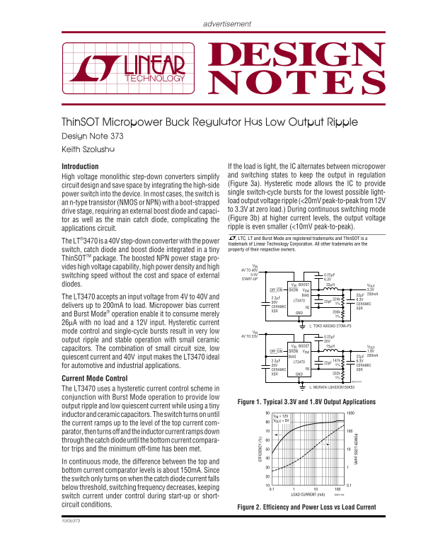
Page 1 Text Content
advertisement
POW ER LOSS (m
Thin SOT Micropower Buck Regulator Has Low Output Ripple Design Note 373 Keith Szolusha
Introduction If the load is light, the IC alternates between micropower and switching states to keep the output in regulation
High voltage monolithic step-down converters simplify
(Figure 3a). Hysteretic mode allows the IC to provide
circuit design and save space by integrating the high-side
single switch-cycle bursts for the lowest possible light-
power switch into the device. In most cases, the switch is
load output voltage ripple (<20m V peak-to-peak from 12V
an n-type transistor (NMOS or NPN) with a boot-strapped
to 3.3V at zero load.) During continuous switching mode
drive stage, requiring an external boost diode and capaci-
tor as well as the main catch diode, complicating the (Figure 3b) at higher current levels, the output voltage ripple is even smaller (<10m V peak-to-peak).
applications circuit.
, LTC, LT and Burst Mode are registered trademarks and Thin SOT is a
The LT®3470 is a 40V step-down converter with the power
trademark of Linear Technology Corporation. All other trademarks are the switch, catch diode and boost diode integrated in a tiny property of their respective owners.
Thin SOTTM package. The boosted NPN power stage pro- EF FI CI EN CY
vides high voltage capability, high power density and high
4V TO 40V 5.5V 0.22µF
switching speed without the cost and space of external
START-UP 6.3V
diodes. VIN BOOST 33µH VOUT
SHDN VSWOFF ON 3.3V BIAS 22µF 200m A
The LT3470 accepts an input voltage from 4V to 40V and 2.2µF 324k
LT3470 6.3V
CERAMIC
delivers up to 200m A to load. Micropower bias current CERAMIC FB
and Burst Mode® operation enable it to consume merely 1% 26µA with no load and a 12V input. Hysteretic current
L: TOKO A003AS-270M=P3
mode control and single-cycle bursts result in very low VIN 4V TO 23V 0.22µF
output ripple and stable operation with small ceramic 25V
VIN BOOST 15µH VOUT
capacitors. The combination of small circuit size, low
SHDN VSWOFF ON 1.8V BIAS 22µF 200m A
quiescent current and 40V input makes the LT3470 ideal
LT3470
25V 1%22p F CERAMIC
for automotive and industrial applications.
CERAMIC FB X5R
X5R GND 332k 1%
Current Mode Control
DN373 F01
L: MURATA LQH32CN150K53
The LT3470 uses a hysteretic current control scheme in conjunction with Burst Mode operation to provide low
Figure 1. Typical 3.3V and 1.8V Output Applications
output ripple and low quiescent current while using a tiny inductor and ceramic capacitors. The switch turns on until VIN = 12V
VOUT = 5V
the current ramps up to the level of the top current com- parator, then turns off and the inductor current ramps down through the catch diode until the bottom current compara- tor trips and the minimum off-time has been met. In continuous mode, the difference between the top and bottom current comparator levels is about 150m A. Since the switch only turns on when the catch diode current falls
below threshold, switching frequency decreases, keeping 0.1
LOAD CURRENT (m A) DN373 F02
switch current under control during start-up or short- circuit conditions.
Figure 2. Efficiency and Power Loss vs Load Current
Page Summary Contents For LINEAR ThinSOT Micropower Buck Regulator Low Output Ripple Design Note 373
Manual Details
| Brand | Linear |
|---|---|
| Pages | 2 |
| File Size | 83.53 KB |
| Published | June 21, 2026 |
Enter the captcha to get the download link:

Frequently Asked Questions
What is the minimum operating voltage range for the LT3470 regulator?
It accepts an input voltage from 4V to 40V.
What is the maximum output ripple achievable in continuous switching mode?
The output ripple can be as low as <10mV peak-to-peak.
How does the LT3470 protect itself from overvoltage when boosting?
It integrates a high side NPN power switch and Schottky catch diode, providing protection for wide input voltage ranges.