LINEAR Driving a Low Noise, Low Distortion 18-Bit, 1.6Msps ADC Design Note 494
Summary
The LTC2379-18 is a high-performance 18-bit, 1.6Msps SAR ADC designed for demanding signal acquisition applications. This technical manual provides comprehensive design notes on optimal integration, presenting multiple advanced driver circuits—including fully differential, single-ended, and power-saving single-supply solutions. It equips engineers with detailed guidance on minimizing noise, achieving ultra-low distortion across various input signals, and implementing critical layout strategies for stable operation in high-speed data systems.
Page 1 Text Content
Driving a Low Noise, Low Distortion 18-Bit, 1.6Msps ADC Design Note 494 Guy Hoover
Introduction the LT®6203 and minimizes disturbances reflected into
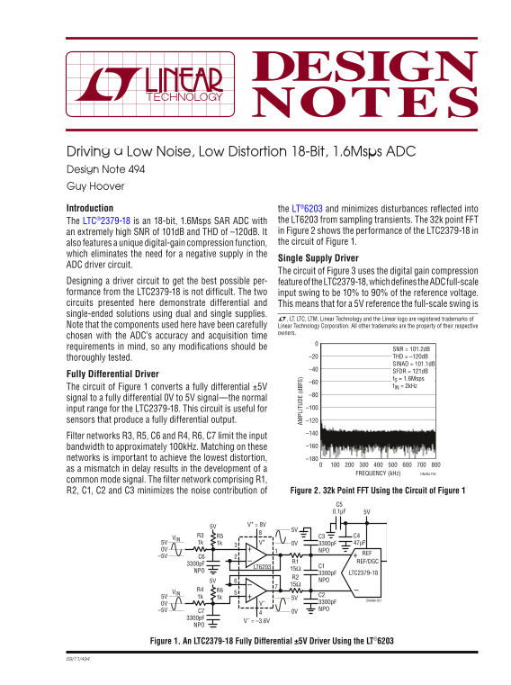
The LTC®2379-18 is an 18-bit, 1.6Msps SAR ADC with the LT6203 from sampling transients. The 32k point FFT an extremely high SNR of 101d B and THD of –120d B. It in Figure 2 shows the performance of the LTC2379-18 in also features a unique digital-gain compression function, the circuit of Figure 1.
which eliminates the need for a negative supply in the
Single Supply Driver
ADC driver circuit.
The circuit of Figure 3 uses the digital gain compression
Designing a driver circuit to get the best possible per- feature of the LTC2379-18, which defines the ADC full-scale formance from the LTC2379-18 is not difficult. The two input swing to be 10% to 90% of the reference voltage.
AM PL IT UD (d BF S)
circuits presented here demonstrate differential and This means that for a 5V reference the full-scale swing is single-ended solutions using dual and single supplies.
L, LT, LTC, LTM, Linear Technology and the Linear logo are registered trademarks of
Note that the components used here have been carefully Linear Technology Corporation. All other trademarks are the property of their respective
owners.
chosen with the ADC’s accuracy and acquisition time requirements in mind, so any modifications should be SNR = 101.2d B
thoroughly tested. –20 THD = –120d B SINAD = 101.1d B
SFDR = 121d B
Fully Differential Driver
f S = 1.6Msps
The circuit of Figure 1 converts a fully differential ±5V f IN = 2k Hz
signal to a fully differential 0V to 5V signal—the normal
input range for the LTC2379-18. This circuit is useful for –100 sensors that produce a fully differential output. –120 –140
Filter networks R3, R5, C6 and R4, R6, C7 limit the input
bandwidth to approximately 100k Hz. Matching on these –160
networks is important to achieve the lowest distortion, –180 as a mismatch in delay results in the development of a
FREQUENCY (k Hz) DN494 F02
common mode signal. The filter network comprising R1,
R2, C1, C2 and C3 minimizes the noise contribution of Figure 2. 32k Point FFT Using the Circuit of Figure 1
0V NPO
R1 REF/DGC
LT6203 C1
3300p F LTC2379-18
5V NPO
DN494 F01
0V V– 3300p F –5V NPO
Figure 1. An LTC2379-18 Fully Differential ±5V Driver Using the LT®6203
Page Summary Contents For LINEAR Driving a Low Noise, Low Distortion 18-Bit, 1.6Msps ADC Design Note 494
Manual Details
| Brand | Linear |
|---|---|
| Pages | 2 |
| File Size | 1.04 MB |
| Published | June 16, 2026 |
Enter the captcha to get the download link:

Frequently Asked Questions
What key specifications define the LTC2379-18 ADC?
It is an 18-bit SAR ADC with a sampling rate of 1.6 Msps, achieving high performance like 101dB SNR and –120dB THD.
Does the LTC2379-18 require a negative supply circuit for operation?
No, it features a unique digital-gain compression function that eliminates the need for a negative supply, allowing single-supply operation.
What layout considerations are important when designing a PCB for this ADC?
You must always use a ground plane, keep analog input traces screened by ground, and ensure bypass capacitors are placed as close as possible to their respective pins.
What is the recommended full-scale swing range for optimal performance?
The two input swing should be between 10% and 90% of the reference voltage.