# A B C D E F G H I J K L M N O P Q R S T U V W X Y Z

LINEAR LTC2248 14-Bit, 65 Msps Low Power 3V ADC Data Sheet

Summary

This comprehensive technical manual details the high-performance LTC2248/LTC2247/LTC2246 series of 14-bit, low-power Analog-to-Digital Converters (ADCs). Designed for demanding signal processing, these converters feature speeds up to 65Msps and exceptional clarity with high SNR and SFDR. The documentation provides full specifications, wiring diagrams, and performance data critical for system integration. Essential for engineers building sophisticated instrumentation in fields such as wireless broadband communication, medical ultrasound, spectral analysis, and advanced imaging systems.
📄 Preview PAGE OF 20

Page 1 Text Content

查询LTC2246供应商

LTC2248/LTC2247/LTC2246

14-Bit, 65/40/25Msps Low Power 3V ADCs

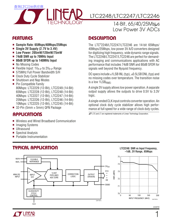
FEATURES DESCRIPTIO Sample Rate: 65Msps/40Msps/25Msps The LTC®2248/LTC2247/LTC2246 are 14-bit 65Msps/ Single 3V Supply (2.7V to 3.4V) 40Msps/25Msps, low power 3V A/D converters designed Low Power: 205m W/120m W/75m W for digitizing high frequency, wide dynamic range signals. 74d B SNR up to 70MHz Input The LTC2248/LTC2247/LTC2246 are perfect for demand- 80d B SFDR up to 140MHz Input ing imaging and communications applications with AC No Missing Codes performance that includes 74d B SNR and 80d B SFDR for Flexible Input: 1VP-P to 2VP-P Range signals well beyond the Nyquist frequency. 575MHz Full Power Bandwidth S/H

DC specs include ±1LSB INL (typ), ±0.5LSB DNL (typ) and

Clock Duty Cycle Stabilizer

no missing codes over temperature. The transition noise

Shutdown and Nap Modes

is a low 1LSBRMS.

Pin Compatible Family

80Msps: LTC2229 (12-Bit), LTC2249 (14-Bit) A single 3V supply allows low power operation. A separate 65Msps: LTC2228 (12-Bit), LTC2248 (14-Bit) output supply allows the outputs to drive 0.5V to 3.3V 40Msps: LTC2227 (12-Bit), LTC2247 (14-Bit) logic.

25Msps: LTC2226 (12-Bit), LTC2246 (14-Bit)

A single-ended CLK input controls converter operation. An

10Msps: LTC2225 (12-Bit), LTC2245 (14-Bit)

optional clock duty cycle stabilizer allows high perfor-

32-Pin (5mm × 5mm) QFN Package

mance at full speed for a wide range of clock duty cycles.

SN (d BF S) , LTC and LT are registered trademarks of Linear Technology Corporation.

APPLICATIO S Wireless and Wired Broadband Communication Imaging Systems Ultrasound Spectral Analysis Portable Instrumentation

TYPICAL APPLICATIO LTC2248: SNR vs Input Frequency, –1d B, 2V Range, 65Msps

FLEXIBLE REFL REFERENCE

14-BIT

ANALOG CORRECTION OUTPUT

INPUT PIPELINED

INPUT LOGIC DRIVERS

S/H ADC CORE

CLOCK/DUTY CYCLE CONTROL

INPUT FREQUENCY (MHZ)

2249 TAO1b

2249 TA01a

Page Summary Contents For LINEAR LTC2248 14-Bit, 65 Msps Low Power 3V ADC Data Sheet

Page 1 查询LTC2246供应商 LTC2248/LTC2247/LTC2246 14-Bit, 65/40/25Msps Low Power 3V ADCs FEATURES DESCRIPTIO Sample Rate: 65Msps/40Msps/25Msps The LTC®2248/LTC2247/LTC2246 are 14-bit 65Msps/ Single 3V Supply (2.7V...
Page 2 LTC2248/LTC2247/LTC2246 ABSOLUTE AXI RATI GS PACKAGE/ORDER I FOR ATIO OVDD = VDD (Notes 1, 2) Supply Voltage (VDD) 4V TOP VIEW ORDER PART Digital Output Ground Voltage (OGND) –0.3V to 1V NUMBER Analog...
Page 3 LTC2248/LTC2247/LTC2246 A ALOG I PUT The ● denotes the specifications which apply over the full operating temperature range, otherwise specifications are at TA = 25°C. (Note 4) SYMBOL PARAMETER CONDIT...
Page 4 LTC2248/LTC2247/LTC2246 I TER AL REFERE CE CHARACTERISTICS (Note 4) PARAMETER CONDITIONS MIN TYP MAX UNITS VCM Output Voltage IOUT = 0 1.475 1.500 1.525 VCM Output Tempco ±30 ppm/C VCM Line Regulation...
Page 5 LTC2248/LTC2247/LTC2246 UW TI I G CHARACTERISTICS The ● denotes the specifications which apply over the full operating temperature range, otherwise specifications are at TA = 25°C. (Note 4) IN ER RO (...
Page 6 CO UN AM PL IT UD (d B) LTC2248/LTC2247/LTC2246 TYPICAL PERFOR A CE CHARACTERISTICS AM PL IT UD (d B) LTC2248: 8192 Point FFT, LTC2248: 8192 Point FFT, f IN = 5MHz, –1d B, 2V Range, f IN = 30MHz, –1d ...
Page 7 IN ER RO (L SB SF DR (d Bc ND BF S) SN AN SF DR (d BF S) LTC2248/LTC2247/LTC2246 TYPICAL PERFOR A CE CHARACTERISTICS LTC2248: SNR and SFDR vs Sample Rate, 2V Range, LTC2248: SNR and SFDR vs LTC2248: S...
Page 8 SF DR (d BF S) AM PL IT UD (d B) AM PL IT UD (d B) LTC2248/LTC2247/LTC2246 TYPICAL PERFOR A CE CHARACTERISTICS LTC2247: 8192 Point FFT, LTC2247: 8192 Point FFT, LTC2247: 8192 Point FFT, f IN = 30MHz, ...
Page 9 AM PL IT UD (d B) IN ER RO (L SB SN (d Bc ND BF S) LTC2248/LTC2247/LTC2246 TYPICAL PERFOR A CE CHARACTERISTICS LTC2247: IOVDD vs Sample Rate, LTC2247: SFDR vs Input Level, LTC2247: IVDD vs Sample Rate...
Page 10 SF DR (d Bc ND BF S) SF DR (d BF S) AM PL IT UD (d B) LTC2248/LTC2247/LTC2246 TYPICAL PERFOR A CE CHARACTERISTICS LTC2246: 8192 Point 2-Tone FFT, f IN = 10.9MHz and 13.8MHz, LTC2246: Grounded Input LT...
Page 11 LTC2248/LTC2247/LTC2246 PI FU CTIO S AIN+ (Pin 1): Positive Differential Analog Input. D0 – D13 (Pins 12, 13, 14, 15, 16, 17, 18, 19, 22, 23, 24, 25, 26, 27): Digital Outputs. D13 is the MSB. AIN- (Pi...
Page 12 LTC2248/LTC2247/LTC2246 FUNCTIONAL BLOCK DIAGRA AIN FIRST PIPELINED SECOND PIPELINED THIRD PIPELINED FOURTH PIPELINED FIFTH PIPELINED SIXTH PIPELINED INPUT ADC STAGE ADC STAGE ADC STAGE ADC STAGE ADC ...
Page 13 LTC2248/LTC2247/LTC2246 APPLICATIO S I FOR ATIO DYNAMIC PERFORMANCE input tone to the RMS value of the largest 3rd order intermodulation product. Signal-to-Noise Plus Distortion Ratio Spurious Free Dy...
Page 14 LTC2248/LTC2247/LTC2246 APPLICATIO S I FOR ATIO DAC to produce a residue. The residue is amplified and disconnected from the input and the held voltage is passed output by the residue amplifier. Succe...
Page 15 LTC2248/LTC2247/LTC2246 APPLICATIO S I FOR ATIO Input Drive Impedance Figure 5 shows a single-ended input circuit. The imped- ance seen by the analog inputs should be matched. This As with all high pe...
Page 16 LTC2248/LTC2247/LTC2246 APPLICATIO S I FOR ATIO For input frequencies above 70MHz, the input circuits of difference amplifier and switching and control circuit. The Figure 6, 7 and 8 are recommended. ...
Page 17 LTC2248/LTC2247/LTC2246 APPLICATIO S I FOR ATIO CLEAN Other voltage ranges in-between the pin selectable ranges SUPPLY can be programmed with two external resistors as shown in Figure 10. An external ...
Page 18 LTC2248/LTC2247/LTC2246 APPLICATIO S I FOR ATIO Table 1. MODE Pin Function DIGITAL OUTPUTS Clock Duty MODE Pin Output Format Cycle Stablizer Digital Output Buffers Straight Binary Off Figure 12 shows ...
Page 19 LTC2248/LTC2247/LTC2246 APPLICATIO S I FOR ATIO on, so that recovery from nap mode is faster than that from to the device as possible (1.5mm or less). A size 0402 sleep mode, typically taking 100 cloc...
Page 20 LTC2248/LTC2247/LTC2246 RELATED PARTS PART NUMBER DESCRIPTION COMMENTS LTC1741 12-Bit, 65Msps ADC 72d B SNR, 87d B SFDR, 48-Pin TSSOP Package LTC1742 14-Bit, 65Msps ADC 76.5d B SNR, 90d B SFDR, 48-Pin...

Manual Details

Brand Linear
Pages 20
File Size 454.80 KB
Published May 30, 2026
72 views

Enter the captcha to get the download link:

captcha

Frequently Asked Questions

What is the typical Signal-to-Noise Ratio (SNR) provided by these ADCs?

They offer a high SNR of 74dB up to a 70MHz input.

Do these converters accommodate different sample rates?

Yes, they are available at three speeds: 65Msps, 40Msps, and 25Msps.

What is the required operational power supply voltage range?

They require a single 3V supply, specifically ranging from 2.7V to 3.4V.

What defines the acceptable analog input voltage window?

The device accepts an Analog Input Voltage Range of 1V to 2V.