LINEAR Upgrade Your Microcontroller ADC to True 12-Bit Performance Design Note DN463
Summary
Upgrade your systems with the LTC236x family, high-performance 12-bit Analog-to-Digital Converters (ADCs). Designed for engineers needing superior accuracy beyond standard microcontroller limits, these precise converters feature adjustable voltage references and output levels. The manual details advanced integration techniques using a reliable SPI interface, guaranteeing low noise, minimum distortion, and exceptional performance across various sample rates. Ideal for professional applications requiring high fidelity measurement without compromising size or power efficiency.
Page 1 Text Content
Upgrade Your Microcontroller ADC to True 12-Bit Performance Design Note DN463 by Guy Hoover Introduction These ADCs are available in tiny 6-lead and 8-lead TSOT-
Many 8-bit and 16-bit microcontrollers feature 10-bit 23 packages. The 8-lead devices have adjustable VREF internal ADCs. A few include 12-bit ADCs, but these often and OVDD pins. The adjustable VREF pin allows the input have poor or nonexistent AC specifi cations, and certainly span to be reduced to 1.4V. This, combined with the high lack the performance to meet the needs of an increasing ADC input impedance, can eliminate the need for gain or number of applications. The LTC®2366 and its slower buffer stages in many applications. The OVDD pin, which speed versions offer a high performance alternative, as controls the digital output level, can be adjusted from 1V shown in the AC specifi cations in Table 1. Compare these to 3.6V, simplifying communication with different logic guaranteed specifi cations with the ADC built into your families. For applications that do not require an adjustable current microcontroller. reference or adjustable output levels, the 6-lead device with VREF = OVDD = VDD should suffi ce.
This family’s DC specifi cations are equally impressive. INL
FO IE FO
and DNL are guaranteed to be less than ±1LSB. Operating The SPI interface requires only three wires to communicate from a single 2.5V, 3V or 3.3V supply, the current draw with the microcontroller, keeping the overall solution size on these parts is a maximum of 4m A during a conver- small in low power, high speed applications.
sion. This can be reduced to less than 1μA by placing L, LT, LTC and LTM are registered trademarks of Linear Technology Corporation.
All other trademarks are the property of their respective owners.
the part into SLEEP mode during periods of inactivity, which greatly reduces the average supply current at lower sample rates.
3.3V 8192 Pt FFT
f S = 2.84MHz –20 VIN = –1d B AT 20k Hz C5 C4 SNR = 72.1d B
R1 0.1μF 10μF –40 THD = –70.1d B 1k R2
1k VDD VREF OVDD
AGND AGND –60
LT6202 AIN LTC2366 SCK
AGND 499Ω
24.9Ω SDO –100
1μF dn463 F01 –120
AGND AV=–4 2.0k
AGND AGND
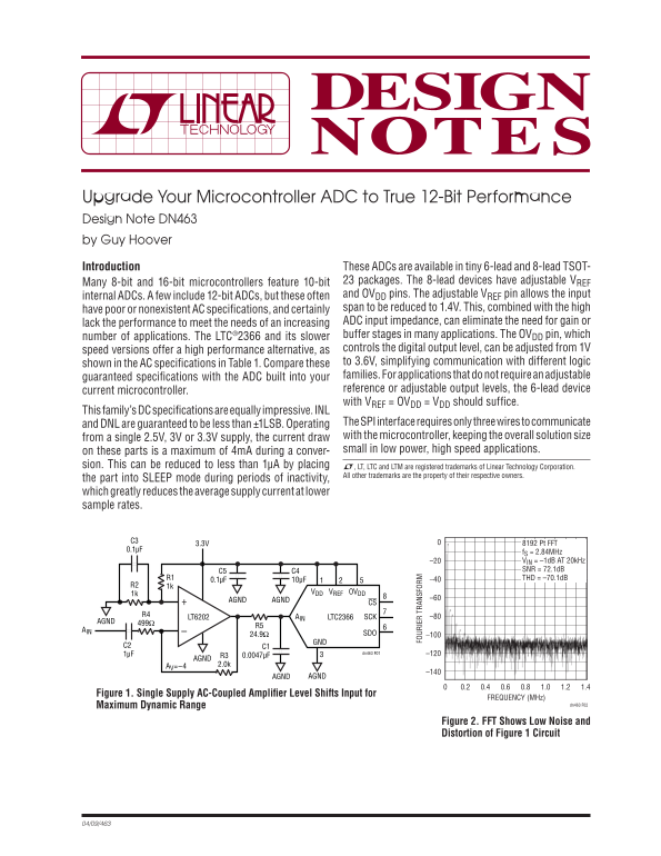
Figure 1. Single Supply AC-Coupled Amplifi er Level Shifts Input for
FREQUENCY (MHz)
Maximum Dynamic Range dn463 F02
Figure 2. FFT Shows Low Noise and Distortion of Figure 1 Circuit
Page Summary Contents For LINEAR Upgrade Your Microcontroller ADC to True 12-Bit Performance Design Note DN463
Manual Details
| Brand | Linear |
|---|---|
| Pages | 2 |
| File Size | 85.42 KB |
| Published | June 18, 2026 |
Enter the captcha to get the download link:

Frequently Asked Questions
What communication interface does this ADC use?
The device uses an SPI interface, which requires only three wires to communicate with a microcontroller.
Can the input or output levels be customized for different systems?
Yes, adjustable V and OV pins allow the ADCs to provide customizable versions of internal references and differential output levels.
How do I improve data quality when dealing with very low signal levels?
Using circuits like the LTC6915 can boost signals, ensuring you achieve full SNR performance from the ADC's dynamic range.
What feature helps conserve power during periods of inactivity?
Placing the part into SLEEP mode during non-usage greatly reduces the average supply current draw.